
Optical data link stably operable for duplicated reset

a technology of optical data link and duplicate reset, applied in the field of optical data link, can solve the problems of further hardware reset asserted and unstable internal serial bus

Inactive Publication Date: 2008-06-05
SUMITOMO ELECTRIC IND LTD
View PDF6 Cites 10 Cited by
  • Summary
  • Abstract
  • Description
  • Claims
  • Application Information

AI Technical Summary

Benefits of technology

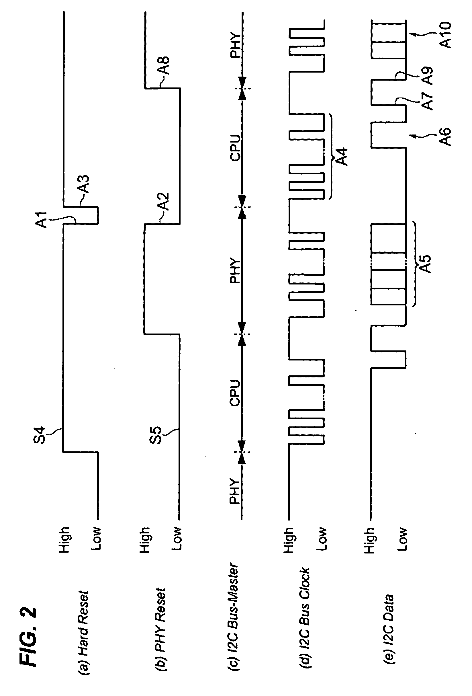
[0011]Because the data left on the data line at the acceptance of the duplicate reset signal may be swept by the dummy clock output from the controller; no data is left on the data line after the step (b) above. Thus, the data link may securely recover from the reset procedure.

Problems solved by technology

When the external apparatus coupled through the external serial communication line requests the internal bus by the software RESET during the initializing process of the data link, a bus collision may occur and accordingly the data link becomes instable.
However, an extreme case may occur in which further hardware RESET is asserted during the initializing process by the software RESET.
The internal serial bus may be unstable for such double resetting procedure, and the conventional data link has provided no means to respond such double requests.

Method used


Image

  • Optical data link stably operable for duplicated reset
  • Optical data link stably operable for duplicated reset
  • Optical data link stably operable for duplicated reset

Examples


Embodiment Construction

[0016]Next, preferred embodiments of the present invention will be described as referring to accompanying drawings.

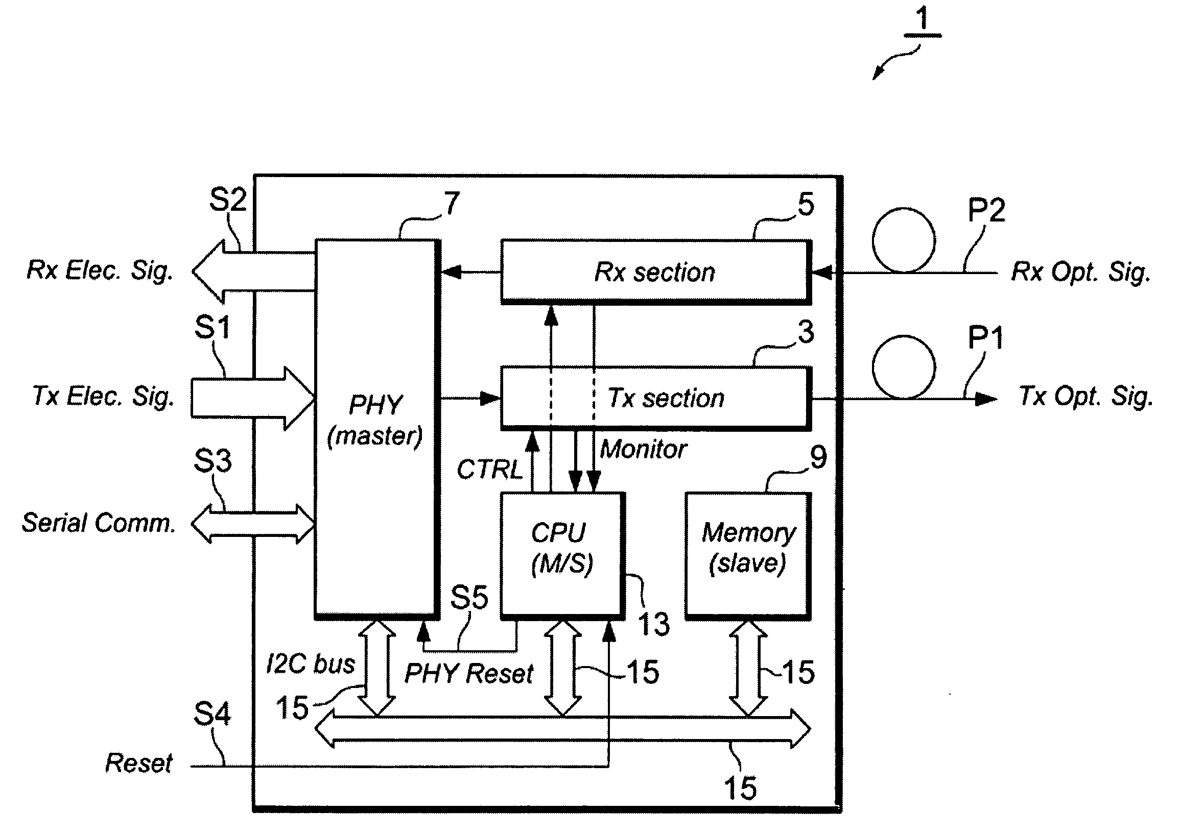
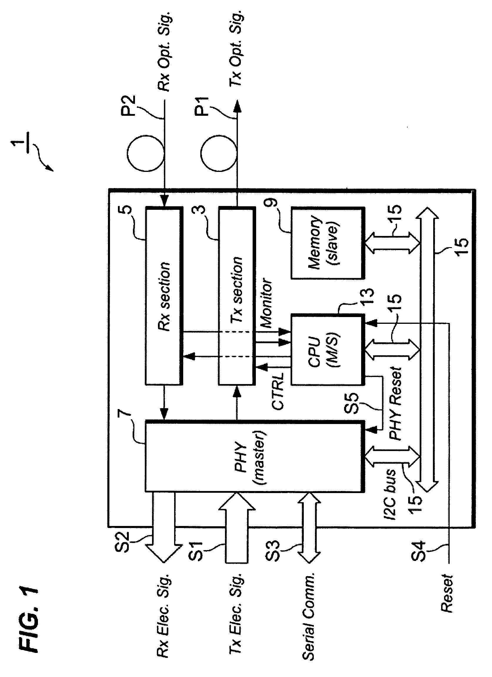
[0017]FIG. 1 illustrates a block diagram of an optical data link according to an embodiment of the invention. The data link shown in FIG. 1, which is coupled with a host system (not shown in FIG. 1), converts a transmitting electrical signal S1 to a transmitting optical signal P1 to output from the transmitter section 3, and converts a receiving optical signal P2 received by the receiver section 5 to a receiving electrical signal S2. The transmitter section 3 includes a transmitter optical subassembly (TOSA) that installs a semiconductor laser diode, while the receiver section 5 includes a receiver optical subassembly (ROSA) that installs a photodiode.

[0018]The data link 1 shown in FIG. 1 further provides an IC 7 configured to manage the communication of the transmitter and receiver sections, 3 and 4, with the external devices, or with the host system, which is often ca...


PUM


Abstract

The preset invention provides an optical data link that prevents the internal I2C bus system from being hung up. The data link provides a CPU able to receive a reset signal and an IC (PHY) to control the physical layer to communicate with the outside of the data link, and they are coupled via the internal I2C bus system. When the data link receives a reset signal, the PHY behaves as the slave device, while, the controller behaves as the master device to output dummy clocks on the clock line of the I2C bus so as to sweep left data on the data line of the I2C bus.

Description

BACKGROUND OF THE INVENTION[0001]1. Field of the Invention[0002]The present invention relates to an optical data link that provides an optical transmitting section and an optical receiving section.[0003]2. Related Prior Art[0004]Japanese Patent Application published as JP-2006-099410A has disclosed an optical data link that provides an IC for controlling a physical layer to communicate with the outside of the data link, which is often denoted as PHY, an electrical erasable programmable memory (EEPROM) that holds data and coupled with the PHY via the internal serial communication bus, and the transmitting and receiving section. In such a data link, initializing the optical transceiver triggered by the RESET provided outside of the data link, the internal serial bus becomes active and the data to be treated in the initializing process are read out from the memory. When the external apparatus coupled through the external serial communication line requests the internal bus by the softwa...

Claims


Application Information

Patent Timeline
IPC IPC(8): H04B10/00G06F13/00H04B10/07H04B10/524H04B10/556
CPCH04B10/40H04B10/278
Inventor ISHIBASHI, HIROTO
Owner SUMITOMO ELECTRIC IND LTD
Learn More