Semiconductor Package and Production Method Thereof, and Semiconductor Device

a technology of semiconductor devices and semiconductors, applied in the direction of semiconductor devices, semiconductor/solid-state device details, electrical apparatus, etc., can solve problems such as variable defects, and achieve the effect of fewer defects

Inactive Publication Date: 2008-06-05
COLLABO INNOVATIONS INC
View PDF2 Cites 18 Cited by
  • Summary
  • Abstract
  • Description
  • Claims
  • Application Information

AI Technical Summary

Benefits of technology

[0029]With a semiconductor package and production method thereof and a semiconductor device of the present invention, highly-reliable semiconductor package or semiconductor device with fewer defects caused by debris of a mold material is realized.

Problems solved by technology

It has been known, however, that the residual resin (or ceramic) has small adhesivity to the leads and therefore readily falls off, thereby causing various defects.

Method used


Image

  • Semiconductor Package and Production Method Thereof, and Semiconductor Device
  • Semiconductor Package and Production Method Thereof, and Semiconductor Device
  • Semiconductor Package and Production Method Thereof, and Semiconductor Device

Examples


embodiment 1

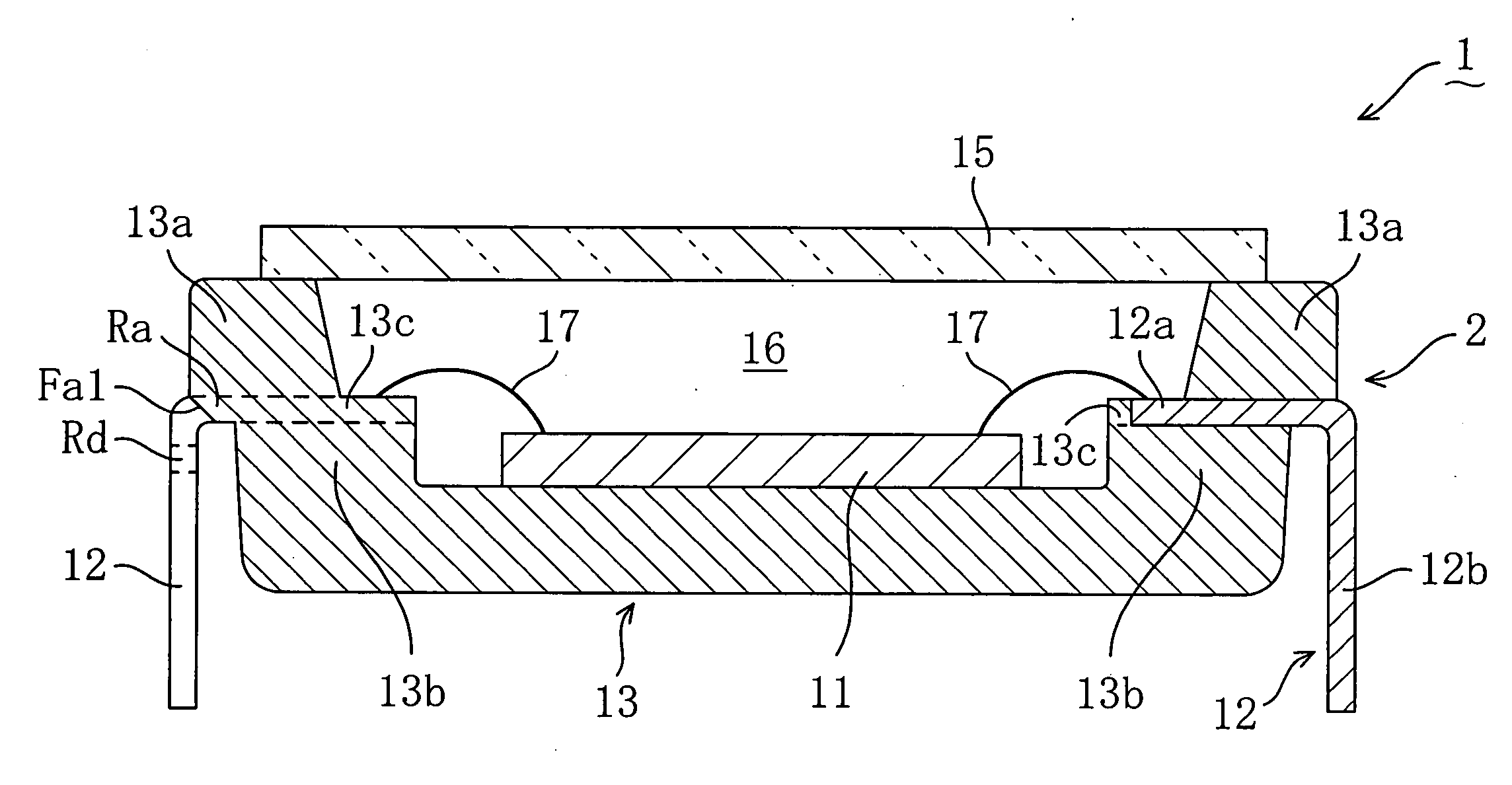
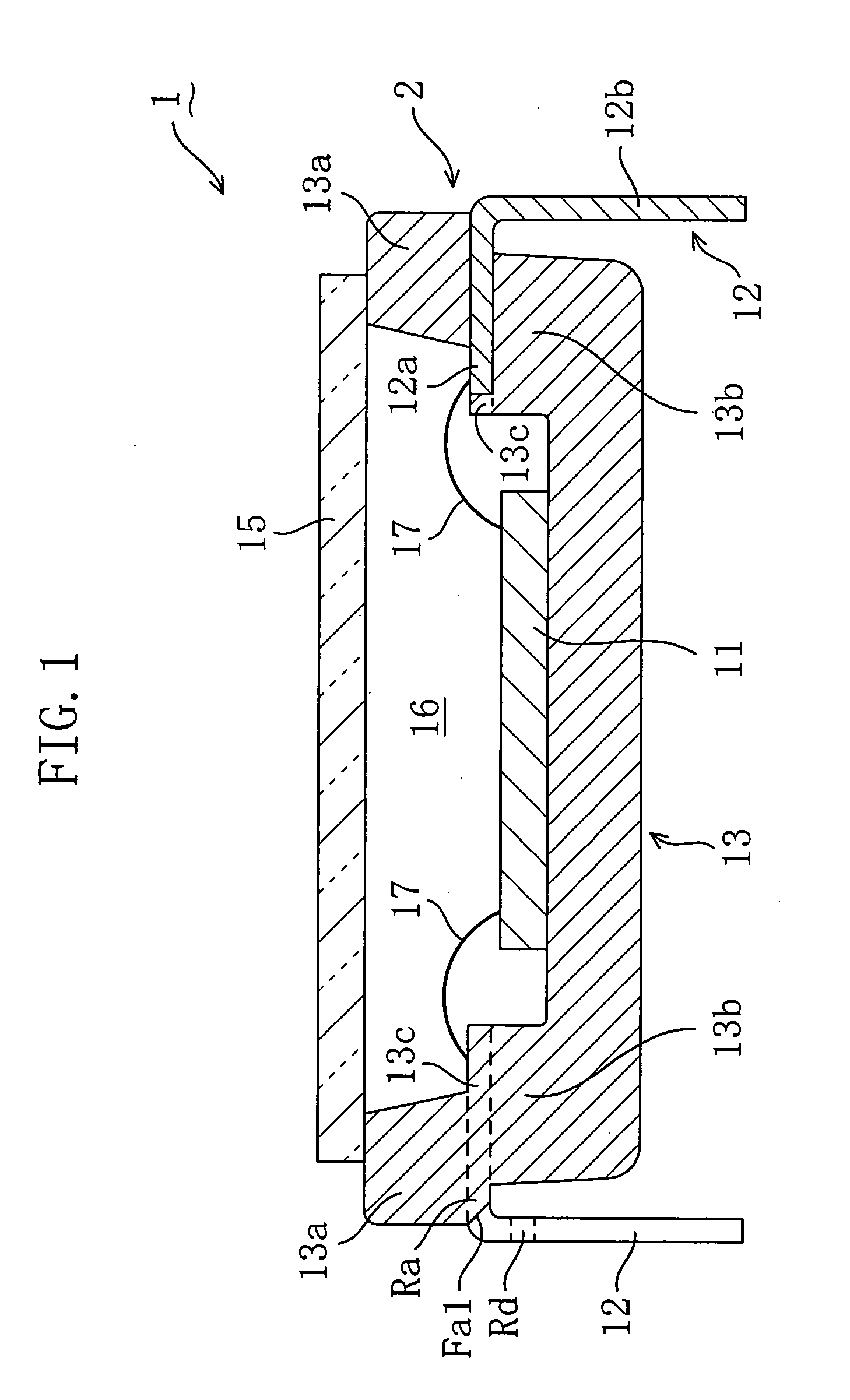
[0072]FIG. 1 is a cross-sectional view showing the structure of a semiconductor device 1 according to embodiment 1 of the present invention. It should be noted that at the left end of FIG. 1, the structure of a cross-section through resin part between leads is shown, while at the right end of FIG. 1, the structure of a cross-section through a lead is shown. As shown in FIG. 1, the optical device 1 includes a semiconductor chip 11, such as a solid state imaging element, light-receiving / emitting element, LSI, or the like, a lead 12 for transmission / reception of a signal between the semiconductor chip 11 and an external device, a metal wire 17 for connecting the semiconductor chip 11 and the lead 12, a rectangular seal 13 for sealing the lead 12, and a lid member 15 attached onto the upper surface of the seal 13, such as a glass window, hologram, ceramic lid, or the like. Part of the seal 13 around the lead 12 (specifically, two side regions) includes an upper seal portion 13a which is...

embodiment 2

[0132]Descriptions in this embodiment are directed not to a contrivance for removing a lead side portion in the partial die cut step but to countermeasures against debris with a contrivance in the structure of a mold die in the mold process.

[0133]FIG. 11(a) and FIG. 11(b) are, respectively, a perspective view and plan view showing only the structure near a die cavity of the lower die half of a mold die of embodiment 2.

[0134]As shown in FIG. 11(a) and FIG. 11(b), dam blocks 51 for filling regions surrounded by inner leads and dam bars of the lead frame are provided on a side of a die cavity 55 of the lower die half 50 of the mold die. The inner surface 51a of the dam block 51 is sloped according to the slanted surface Fa of the tip region Ra of the lower seal portion 13b described in embodiment 1.

[0135]FIG. 12(a) and FIG. 12(b) are, respectively, a partial cross-sectional view illustrating the positional relationship between the mold die and the lead frame in the mold step, and a par...


PUM


Abstract

A method of producing semiconductor packages includes the step of punching out a dam-bar and part of the region lateral to a lead of a scaling body formed by molding, the punching-out being effected by using a support block and a punch. The support block has an outer lateral surface in a region receding as much as possible from the lateral surface of the upper portion of the seal body and also has an inner lateral surface almost flush with the lateral surface of the lower portion of the seal body. The width (Wa) of the upper surface of the support block is smaller than the overhang quantity of the upper portion of the seal body. In the region lateral to the lead, the front end region (Ra) positioned immediately below the overhang section of the upper portion of the seal body has an inclined surface (Fa1) sloping inwardly downward.

Description

TECHNICAL FIELD[0001]The present invention relates to a semiconductor package formed of a resin or ceramic, to which an LSI chip, solid state imaging element, light-receiving / emitting element, or the like, is to be mounted, a production method thereof, and a semiconductor device.BACKGROUND ART[0002]Conventionally, the mold step for a semiconductor package has been carried out in such a manner that, in a region adjacent to a die cavity, a lead frame which has leads and dam bars connecting the leads is sandwiched between the lower die half and upper die half of the mold die, and a resin or ceramic is injected into the die cavity for molding.[0003]In this process, as shown in FIG. 3 and FIG. 4 of patent Document 1, resin, or the like, remains between the dam bar and a seal. This is because, in the mold step, the dam bar is positioned outwardly away from the die cavity by a predetermined distance, so that the resin, or the like, leaks in a space surrounded by the upper and lower die hal...

Claims


Application Information

Patent Timeline
Patent Type & Authority Applications(United States)
IPC IPC(8): H01L21/98
CPCH01L21/4842H01L23/057H01L23/49861H01L2924/09701H01L2224/48091H01L2224/48247H01L2924/00014
Inventor INAO, HISAHOHIRANO, TATSUYASHIMIZU, KATSUTOSHI
Owner COLLABO INNOVATIONS INC
Why Eureka
Try Eureka