
Fast on-chip decoupling capacitance budgeting method and device for reduced power supply noise

Inactive Publication Date: 2008-06-05
NXP USA INC
View PDF3 Cites 6 Cited by
  • Summary
  • Abstract
  • Description
  • Claims
  • Application Information

AI Technical Summary

Problems solved by technology

As the design and layout of semiconductor circuits, or microcircuits, or chips, become more complex, and in particular, as there is an increase in complexity of very large scale integration (VLSI) layout, an increase in operational frequency and the use of supply voltage scaling, there is an ever increasing need to remove or reduce undesired noise from the semiconductor circuit design.
A chip's power distribution network is a major noise source as the fluctuations in supply voltage due to the parasitic resistance, inductance and capacitance in the network alter signals' voltage levels and can cause malfunctioning of the chip's circuits.
Designing a robust power distribution network for low dynamic voltage fluctuations has become a challenging task.
Extremely dense and complex circuit layouts for high frequency operation necessitate reduction of these undesired noise levels, especially at some sensitive parts of circuits such as clock generators and analog circuits.
Problematically, the high leakage current in these technology nodes discourages the addition of abundant decoupling capacitance.
As understood in the art, decap budgeting and placement is a non-linear optimization problem.
Its application is thus limited to regular mesh structures.
All these known methods, concepts and techniques, however, are problematic.
Further complicating the problem, these techniques add decap and recompute sensitivity in an iterative procedure.
As the complexity of one adjoint sensitivity computation is the same as one transient analysis, the iterative nonlinear optimization procedure becomes quite expensive and time consuming.
In addition, the adjoint sensitivity calculation typically needs to store waveforms at every node in both the original and the adjoint networks, which may exhaust the memory resource for large networks.
However, the parasitic capacitance and existing decap value are not considered in these methods, which causes inaccuracies.

Method used


Image

  • Fast on-chip decoupling capacitance budgeting method and device for reduced power supply noise
  • Fast on-chip decoupling capacitance budgeting method and device for reduced power supply noise
  • Fast on-chip decoupling capacitance budgeting method and device for reduced power supply noise

Examples


Embodiment Construction

[0015]In the following detailed description of exemplary embodiments of the invention, specific exemplary embodiments in which the invention may be practiced are described in sufficient detail to enable those skilled in the art to practice the invention, and it is to be understood that other embodiments may be utilized and that logical, architectural, programmatic, mechanical, electrical and other changes may be made without departing from the spirit or scope of the invention. The following detailed description is, therefore, not to be taken in a limiting sense, and the scope of the invention is defined only by the appended claims.

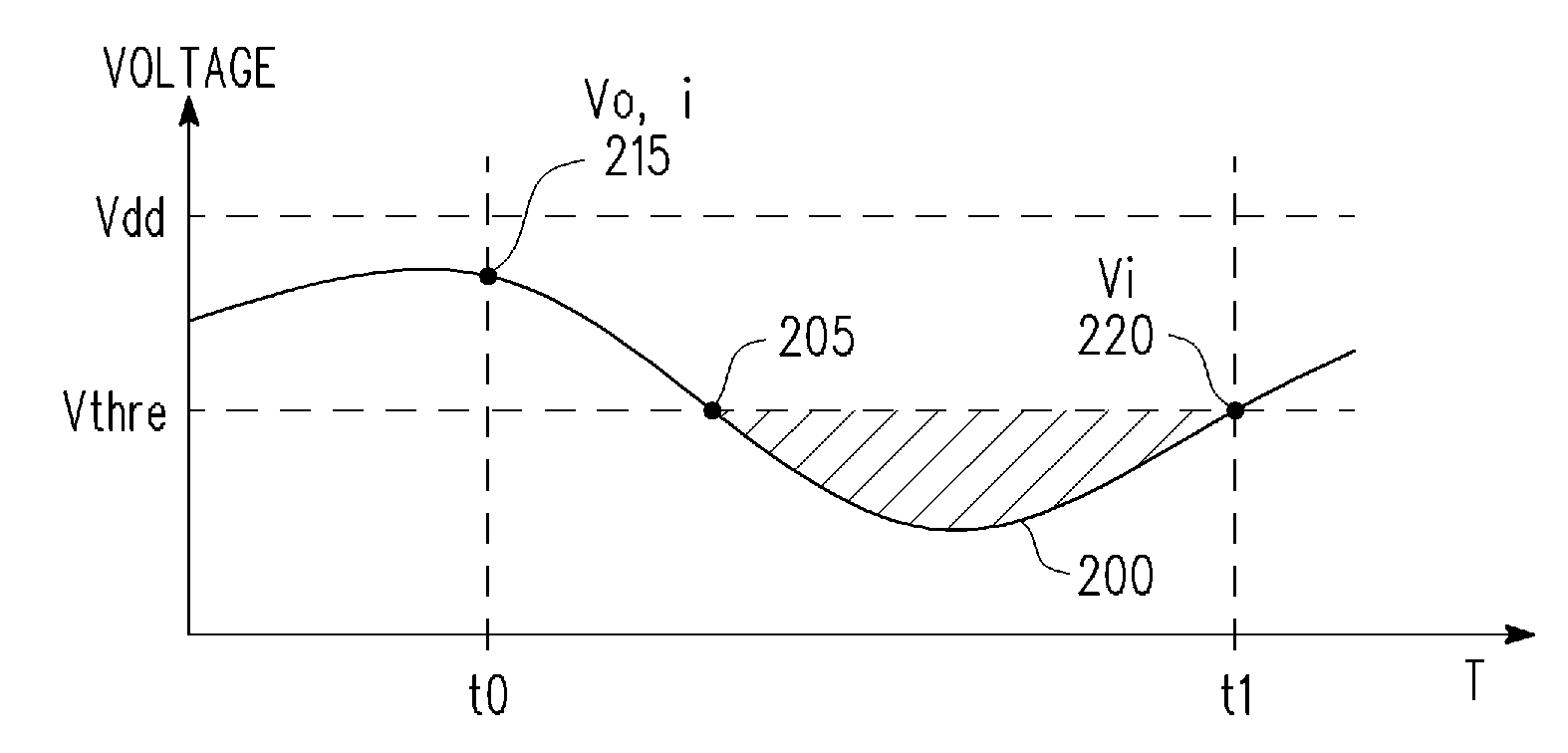
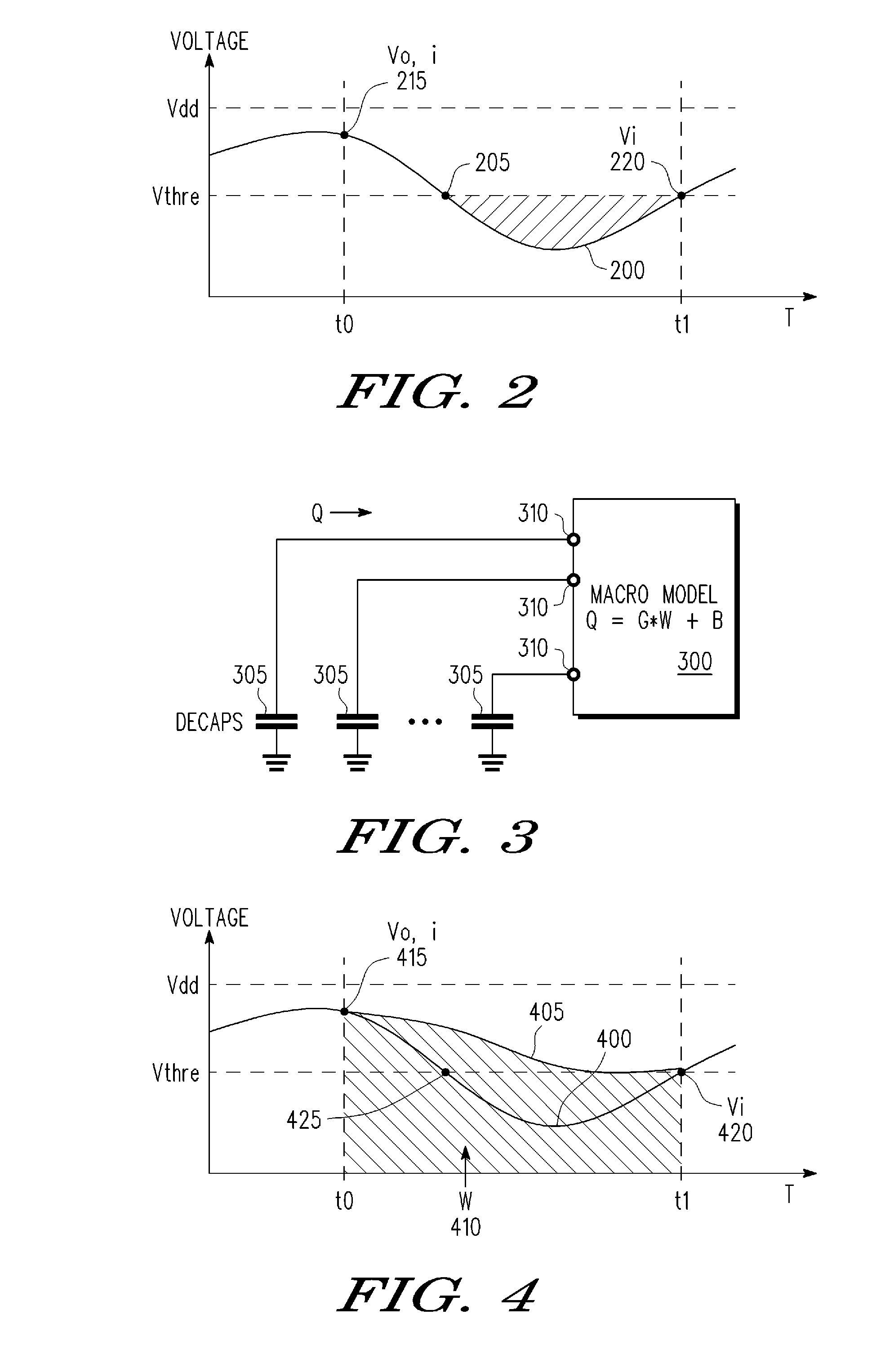
[0016]The method of the preferred embodiment eliminates the problems of the techniques found in the prior art and determines the optimal amount of and the location for decaps, to reduce dynamic supply noise in a circuit quickly and accurately. The method of the preferred embodiment proposes a novel and efficient charge-based decoupling capacitor budgeting ...


PUM


Abstract

A semiconductor power network decoupling capacitance (decap) budgeting problem is formulated to minimize the total decap to be added to the network subject to voltage constraints on the network nodes of a semiconductor circuit design. Voltage constraints on the decap to be added are taken into consideration such that the decap can be distributed throughout a hot spot region of the semiconductor circuit design and not be limited to placement at a single location in the circuit. Dynamic network voltages are at all times maintained greater than a user-specified threshold voltage level.

Description

BACKGROUND OF THE INVENTION[0001]1. Field of the Invention[0002]The invention relates generally to a device and method of determining the value and location of a decoupling capacitance to be added during the design and layout of a semiconductor circuit to optimally reduce dynamic supply voltage fluctuations during circuit operation at high frequency.[0003]2. Description of the Related Art[0004]As the design and layout of semiconductor circuits, or microcircuits, or chips, become more complex, and in particular, as there is an increase in complexity of very large scale integration (VLSI) layout, an increase in operational frequency and the use of supply voltage scaling, there is an ever increasing need to remove or reduce undesired noise from the semiconductor circuit design. A chip's power distribution network is a major noise source as the fluctuations in supply voltage due to the parasitic resistance, inductance and capacitance in the network alter signals' voltage levels and can ...

Claims


Application Information

Patent Timeline
IPC IPC(8): G06F17/50
CPCG06F2217/78G06F17/5036G06F2119/06G06F30/367
Inventor ZHAO, MINPANDA, RAJENDRAN V.SUNDARESWARAN, SAVITHRI
Owner NXP USA INC
Features
  • Generate Ideas
  • Intellectual Property
  • Life Sciences
  • Materials
  • Tech Scout
  • Unparalleled Data Quality
  • Higher Quality Content
  • 60% Fewer Hallucinations
Learn More