
Manufacturing Process For Producing Narrow Sensors

Inactive Publication Date: 2008-06-12
NOVO NORDISK AS
View PDF8 Cites 60 Cited by
  • Summary
  • Abstract
  • Description
  • Claims
  • Application Information

AI Technical Summary

Benefits of technology

[0021]Further, it is an object of the present invention to provide a method of producing an electrode assembly enabling a reduction of the width of the electrode assembly and to provide an electrode assembly having a reduced width.
[0085]In one embodiment, the method comprises: applying the first dielectric layer by applying a first polymer laminate, and applying at least one additional dielectric layer using a printing technique. In this way one dielectric layer is a laminate while at least another may be made using the simple printing technique.

Problems solved by technology

A problem with the present 2D technologies is that if the sensor should be narrow, the conductors down to the electrode areas will take up valuable space on the limited area, see e.g. FIG. 4, which will be explained later.
Additionally, while conventional printing techniques using normal 2D techniques typically offer simple and efficient production of electrodes, it is often a problem to print very fine structures using conventional printing techniques using high viscous printing paste.
Generally, the finer structures (typically below 100 μm line space definition) that can be printed, the more complicated and expensive technique is needed for manufacturing.
As an example, in order to obtain a line space definition in a range about 20 μm, expensive photolithography with sputter deposition manufacturing is needed.
Although the dimensions that can be realised with printing are not as small as with thin-film technology, the ease of use printing technology is very attractive for the production of in-vitro sensors, where the over-all size of the electrode assembly is not a problem and hence the limited capability for printing small structures is in general not recognized.
However, if the electrode assembly is made for an implantable sensor then size will be of great importance since implantation of large sensors will result in a high level of tissue damage as well as a possible formation of scar tissue.
Furthermore, implantation will result in unacceptable pain during insertion.
Although this might potentially reduce the width of a two-electrode assembly to half width, the width reduction for a three-electrode system is relatively limited.
Furthermore experiments have shown that production of double sided foils is not straightforward for a number of different reasons depending on the deposition method chosen.
If the electrode assembly is disposed using a printing technique, aligned double sided prints are not easily achieved due to the nature of the printing process.
If the electrode assembly is formed by etching deposited continuous metal films (thin film technology) it is typically a problem that foils having a suitable metallization on both sides are not readily available.
Furthermore, the subsequent electrochemical modification of the different electrodes has proven to be very complex.

Method used


Image

  • Manufacturing Process For Producing Narrow Sensors
  • Manufacturing Process For Producing Narrow Sensors
  • Manufacturing Process For Producing Narrow Sensors

Examples


Embodiment Construction

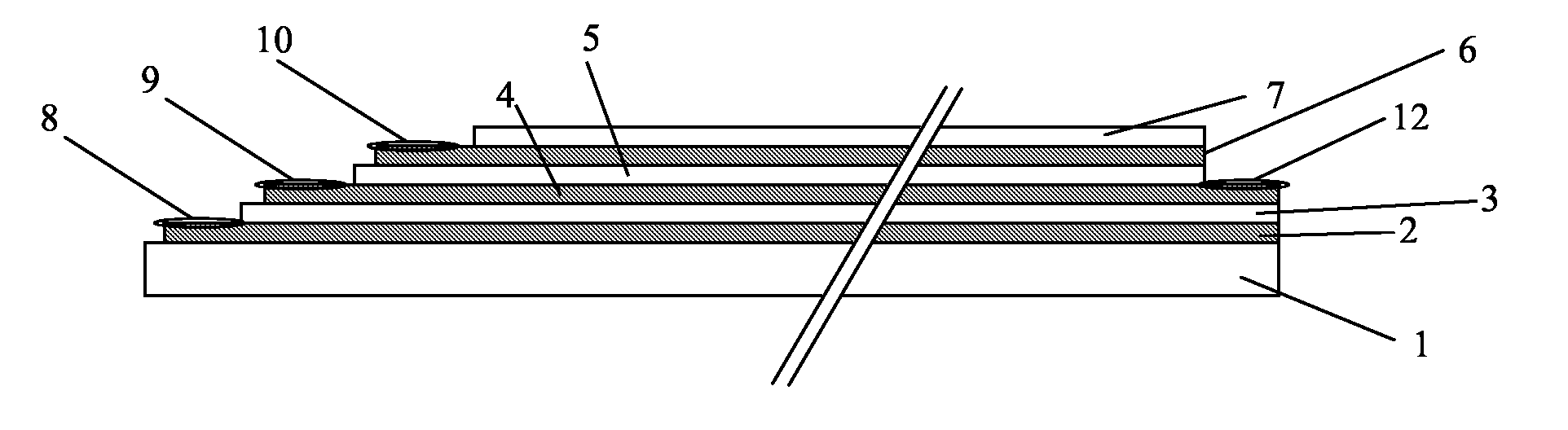
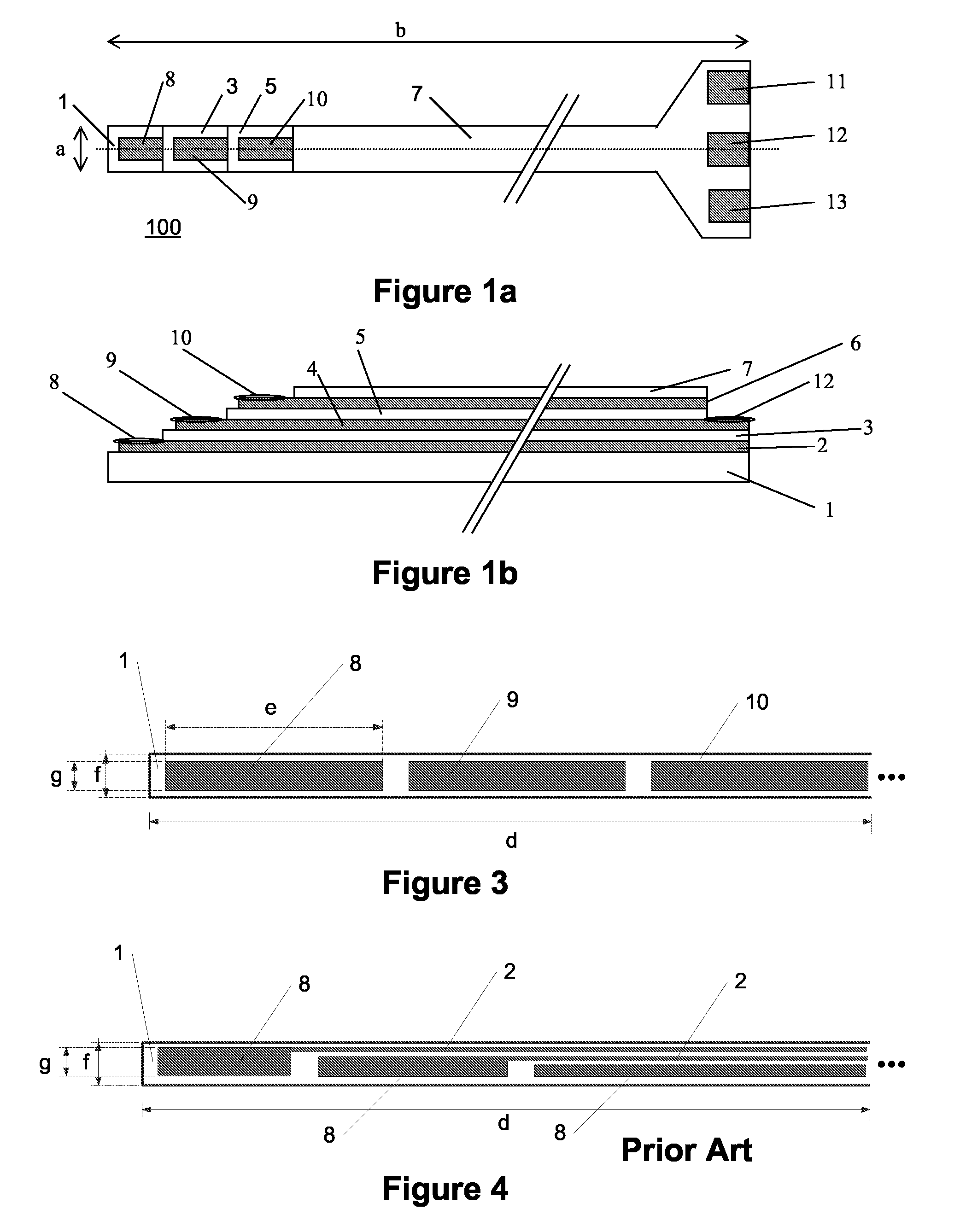
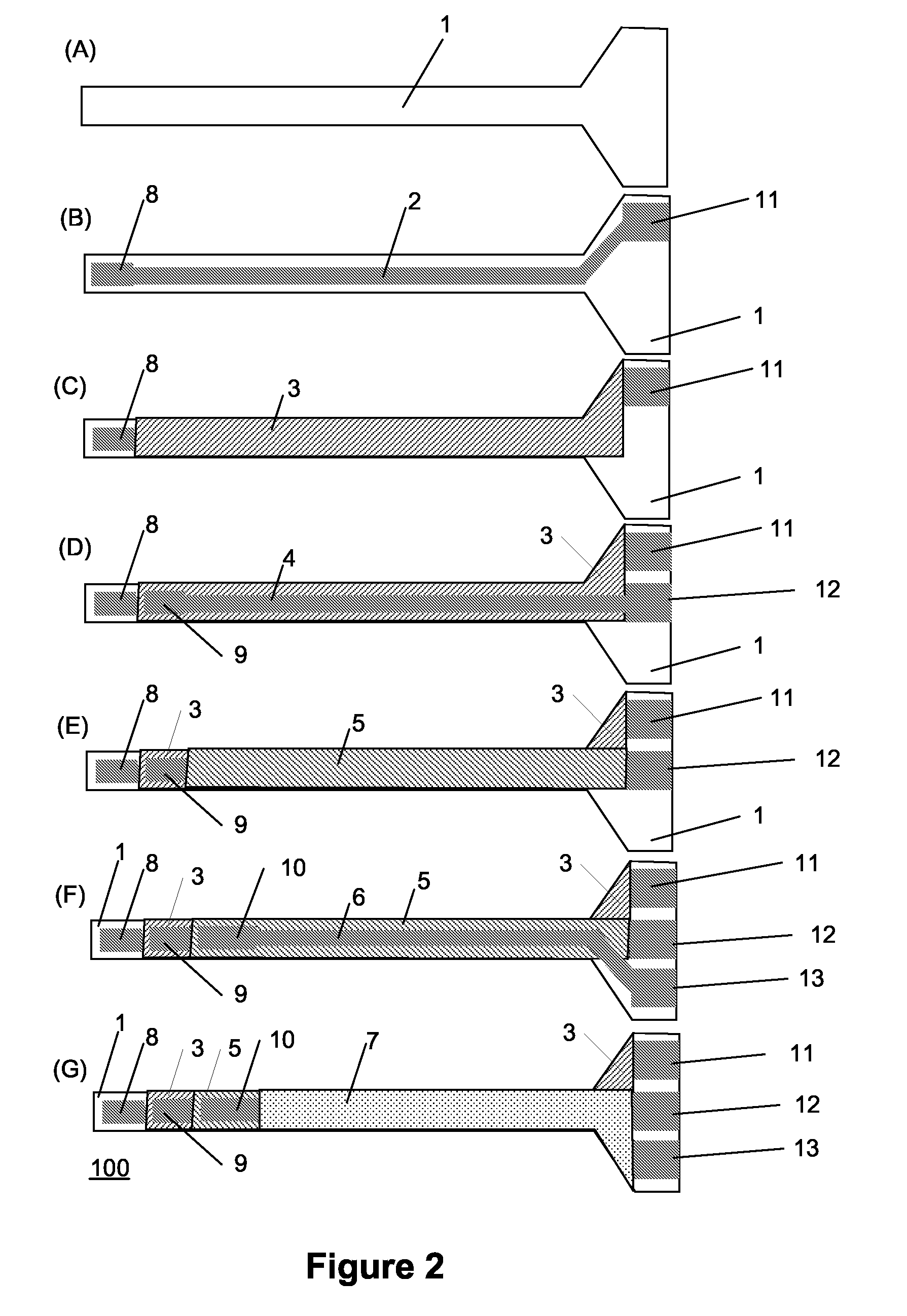
[0098]FIG. 1a schematically illustrates a top view of a (three-)electrode assembly / architecture according to one embodiment of the present invention. Shown is an electrode assembly (100) comprising a dielectric substrate (1), a first electrode surface (ES) (8) of a first conductive layer, a first dielectric layer (3), a second ES (9) of a second conductive layer, a second dielectric layer (5), a third ES (10) of a third conductive layer, a contact pad for electronics (CPE) (11) of the first conductive layer, a CPE (12) of the second conductive layer, a CPE (13) of the third conductive layer, and a third dielectric layer (7).

[0099]The first, second and third conductive layer is not shown specifically but is shown e.g. in FIGS. 1b and 2, as (2), (4) and (6), respectively.

[0100]A single electrode typically comprises a conductive layer comprising an ES, a CPE and a conductive track connecting the ES to the CPE. In the shown embodiment, electrical contact is preferably at the two ends of...


PUM

PropertyMeasurementUnit
Percent by massaaaaaaaaaa

Abstract

This application relates to electrode assemblies (100) for use in an electrochemical sensor, the electrode assembly comprising: a first conductive layer (2) comprising a first electrode surface (8) and a first contact area (11), a second conductive layer (4) comprising a second electrode surface (9) and a second contact area (12), and a first dielectric layer (3) where said first dielectric layer is adjacent to said first conductive layer, wherein said second conductive layer and said first dielectric layer do not cover at least a part of the first and at least a part of the second electrode surface and do not cover at least a part of the first and at least a part of the second contact area. It also relates to methods of manufacturing such electrode assemblies. In this way, modification of conventional 2D structures into sandwiched or 3D structures containing at least two separated conductive layers is provided by a sequential application of further layers constituting at least one dielectric layer and one further conducting layer to the original 2D structure. The dielectric layer may be applied first, followed by the application of a further electrical conducting layer. Alternatively the conventional 2D layer may be modified by lamination of a further 2D layer, thus forming a sandwiched structure.

Description

FIELD OF INVENTION[0001]This invention relates to the production of electrode assemblies suitable for use in electrochemical sensors, in particular transcutaneous electrochemical sensors suitable for in vivo measurement of metabolites.BACKGROUND OF THE INVENTION[0002]In recent years, a variety of electrochemical sensors have been developed for in vivo measurements of metabolites. Most prominent among these glucose sensors have been developed for use in obtaining an indication of blood glucose (BG) levels in a diabetic patient. BG information is of the utmost importance to diabetics, as these readings are instrumental in the adjustment of the treatment regimen. The conventional way to obtain BG information is applying minute amounts of blood to test strips. A new development is transcutaneous sensors where the sensor is implanted under the skin. As the sensor is in contact with biological fluids for a prolonged period of time the possibility for continuous measurements is opened. Con...

Claims


Application Information

Patent Timeline
IPC IPC(8): G01N27/30B05D5/12A61B5/296
CPCA61B5/1468A61B5/14532
Inventor SJOLANDER, ANNIKA LINDGREN
Owner NOVO NORDISK AS
Features
  • Generate Ideas
  • Intellectual Property
  • Life Sciences
  • Materials
  • Tech Scout
  • Unparalleled Data Quality
  • Higher Quality Content
  • 60% Fewer Hallucinations
Learn More