Semiconductor device and method for manufacturing same

a technology of semiconductor devices and semiconductors, applied in semiconductor devices, semiconductor/solid-state device details, electrical apparatus, etc., can solve the problems of production costs increasing and production costs increasing, and achieve the effect of cost effectiveness

Active Publication Date: 2008-06-12
DENSO CORP
View PDF9 Cites 57 Cited by
  • Summary
  • Abstract
  • Description
  • Claims
  • Application Information

AI Technical Summary

Benefits of technology

[0010]In view of the above and other problems, the present disclosure provides a semiconductor device and a method for manufacturing the device that has plural active elements or

Problems solved by technology

On the other hand, the semiconductor device 90 made of the SOI board 1 with two substrates pasted together has factors such as an increased number of processing steps for die-mounting, implementing as a package and the like, which leads to production costs increase.
On this account, the SOI board having the buried oxide film is used as a device such as a vertical metal oxide semiconductor transistor element and an IGBT element for large curre

Method used


Image

  • Semiconductor device and method for manufacturing same
  • Semiconductor device and method for manufacturing same
  • Semiconductor device and method for manufacturing same

Examples


Embodiment Construction

[0030]The best form to carry out the present invention as follows is explained based on the drawing.

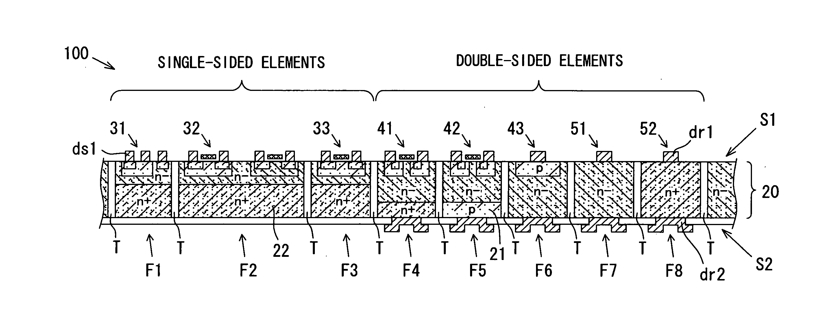
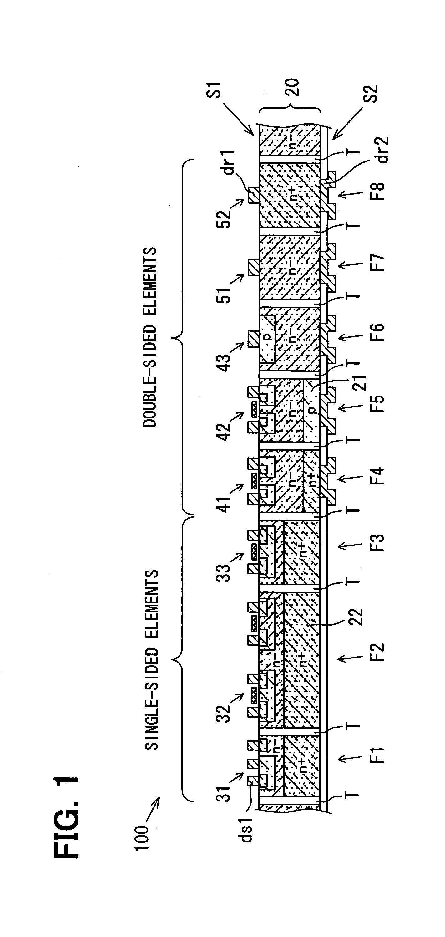
[0031]FIG. 1 is an illustration showing a section of a semiconductor device 100 in an embodiment of the semiconductor device of the present invention.

[0032]The semiconductor device 100 has active elements 31-33, 41-43 and passive elements 51, 52 formed on one the semiconductor substrate 20. In the semiconductor device 100, active elements are exemplarily represented as a bipolar transistor element 31, a complementary MOS (CMOS, Complementary Metal Oxide Semiconductor) transistor element 32, a horizontal metal oxide semiconductor (MOS) transistor element 33, a vertical metal oxide semiconductor (MOS) transistor element 41, an IGBT (Insulated Gate Bipolar Transistor) element 42 and a diode element 43 is exemplified as a masterpiece of the active element. In addition, passive elements are exemplarily represented as an N conductivity type (n−) low impurity density element 51 to be used as...


PUM


Abstract

A semiconductor device having plural active and passive elements on one semiconductor substrate is manufactured in the following cost effective manner even when the active and passive elements include double sided electrode elements. When the semiconductor substrate is divided into plural field areas, an insulation separation trench that penetrates the semiconductor substrate surrounds each of the field areas, and each of the either of the plural active elements or the plural passive elements. Further, each of the plural elements has a pair of power electrodes for power supply respectively disposed on each of both sides of the semiconductor substrate to serve as the double sided electrode elements.

Description

CROSS REFERENCE TO RELATED APPLICATION[0001]This application is based on and claims the benefit of priority of Japanese Patent Application No. 2006-329858 filed on Dec. 6, 2006, and No. 2007-265766 filed on Oct. 11, 2007, the disclosure of which is incorporated herein by reference.FIELD OF THE DISCLOSURE[0002]The present disclosure generally relates to a semiconductor device having plural elements on one substrate and method for manufacturing the device.BACKGROUND INFORMATION[0003]A semiconductor device having a metal oxide semiconductor (MOS) transistor and a bipolar transistor formed on one semiconductor substrate is disclosed, for example, in Japanese Patent Laid-Open No. 2001-60634 (Patent literature 1: U.S. Pat. No. 6,365,932 B1). FIG. 15 is a conventional semiconductor device disclosed in Patent literature 1 for illustrating a section of a semiconductor device 90.[0004]The semiconductor device 90 shown in FIG. 15 is a composite IC that an active element and a passive element a...

Claims


Application Information

Patent Timeline
IPC IPC(8): H01L27/088H01L21/762
CPCH01L21/8221H01L25/074H01L27/0694H01L23/481H01L2924/0002H01L2924/00
Inventor OZEKI, YOSHIHIKOKOUNO, KENJIFUJII, TETSUO
Owner DENSO CORP
Why Eureka
Try Eureka