Method of fabricating bipolar transistors and high-speed lvds driver with the bipolar transistors

a technology of bipolar transistors and drivers, applied in the direction of pulse generators, pulse techniques, digital transmission, etc., can solve the problems of voltage loss, insufficient static current use in i/o applications, and a ratio of width,

Inactive Publication Date: 2008-06-12
ELECTRONICS & TELECOMM RES INST
View PDF32 Cites 16 Cited by
  • Summary
  • Abstract
  • Description
  • Claims
  • Application Information

AI Technical Summary

Problems solved by technology

A CMOS process is generally used to minimize power consumption of the transistors 211, 212, 213 and 214 as switching devices of the driving stage, but it has a disadvantage in that the rated current capacity of the MOS transistor is fully dependent on size (a ratio of width to length; W / L) of the device.
When considering more advanced and diversified I / O interface environments, it may be insufficient to use a static current larger than 7 mV in I / O applications.
Although there is a way of extending a permissible capacity of the rated current by enlarging the size (W / L) of the transistor device, it may cause voltage loss due to signal delay and parasitic resistance, which may result in limitation of signal swing level and an increase of the power source voltage.
However, it also causes enlargement of a device area of layout, increasing parasitic capacitance and generating an output delay.
As a result, enlarging a chip area becomes a problem.

Method used


Image

  • Method of fabricating bipolar transistors and high-speed lvds driver with the bipolar transistors
  • Method of fabricating bipolar transistors and high-speed lvds driver with the bipolar transistors
  • Method of fabricating bipolar transistors and high-speed lvds driver with the bipolar transistors

Examples


Embodiment Construction

[0027]Hereinafter, exemplary embodiments of the present invention will be described in detail. However, the present invention is not limited to the embodiments disclosed below, but can be implemented in various forms. Therefore, the following embodiments are described in order for this disclosure to be complete and enabling to those of ordinary skill in the art.

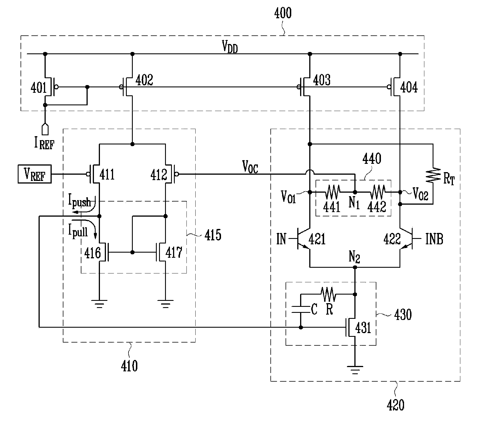
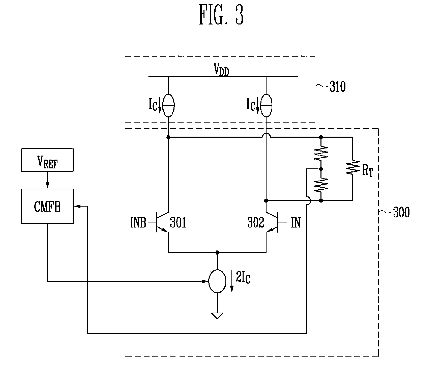
[0028]FIG. 3 is a circuit diagram of a high-speed low-voltage differential signal (LVDS) driver according to an exemplary embodiment of the present invention.

[0029]Referring to FIG. 3, a current source circuit 310 for supplying current to a differential driving circuit 300 in a CMOS process is formed of double current sources (DCSs). In the differential driving circuit 300, the FETs used in the conventional driving circuit are replaced by bipolar transistors 301 and 302.

[0030]Owing to this structural feature, it is possible to minimize parasitic resistance regardless of a size of the device included in the differential-signal...


PUM


Abstract

Provided is a differential signal driver capable of operating at a high speed at a low voltage of 1.8V. The differential signal driver includes: a differential-signal driving circuit for switching input differential signals and outputting a common mode voltage through first and second output nodes; and a common-mode feedback circuit for providing a predetermined current to the differential-signal driving circuit or receiving a predetermined current from the differential-signal driving circuit in response to the common mode voltage. The differential-signal driving circuit includes a common-mode voltage output circuit for connecting the first output node to the second output node and generating the common mode voltage of the differential-signal driving circuit. The differential input signals are received through two bipolar transistors.

Description

CROSS-REFERENCE TO RELATED APPLICATION[0001]This application claims priority to and the benefit of Korean Patent Application Nos. 2006-122932, filed Dec. 6, 2006 and 2007-57137, filed Jun. 12, 2007, the disclosures of which are incorporated herein by reference in their entirety.BACKGROUND[0002]1. Field of the Invention[0003]The present invention relates to differential signal drivers, and more particularly, to a differential signal driver capable of operating at a high speed at a low voltage and bipolar transistors used in the differential signal driver.[0004]The present invention has been produced from the work supported by the IT R&D program of MIC (Ministry of Information and Communication) / IITA (Institute for Information Technology Advancement) [2005-S-073-02, Development of semiconductor circuit design based on the nano-scaled device] in Korea.[0005]2. Discussion of Related Art[0006]Conventionally, a differential data transfer mode transfers data via a transfer signal made from...

Claims


Application Information

Patent Timeline
Patent Type & Authority Applications(United States)
IPC IPC(8): H03K3/00H01L21/8249
CPCH01L21/8249H04L25/0282H01L29/41708H01L29/7322H03F3/45085H03F3/45179H03F3/45502H03F2203/45008H03F2203/45082H03F2203/45418H03F2203/45424H03K5/003H03K19/01H04L25/0276H01L27/0623
Inventor KIM, KWI DONGKWON, CHONG KIKIM, JONG DAE
Owner ELECTRONICS & TELECOMM RES INST
Why Eureka
Try Eureka