Liquid crystal display device and electronic apparatus

Inactive Publication Date: 2008-06-12
JAPAN DISPLAY INC
View PDF5 Cites 14 Cited by
  • Summary
  • Abstract
  • Description
  • Claims
  • Application Information

AI Technical Summary

Benefits of technology

[0072]According to the embodiments of the invention, a difference in operation modes in the transmission area and the reflection area is electrically compensated with a simple structure. It is possible

Problems solved by technology

Therefore, the state of black display is not close to the ideal cross-nicol state in which the liquid crystal layer is not held between the sheet polarizers.
However, in both the patent documents, the structure and a manufacturing process of the liquid crystal display devices are complicated and problems still remain i

Method used


Image

  • Liquid crystal display device and electronic apparatus
  • Liquid crystal display device and electronic apparatus
  • Liquid crystal display device and electronic apparatus

Examples


Example

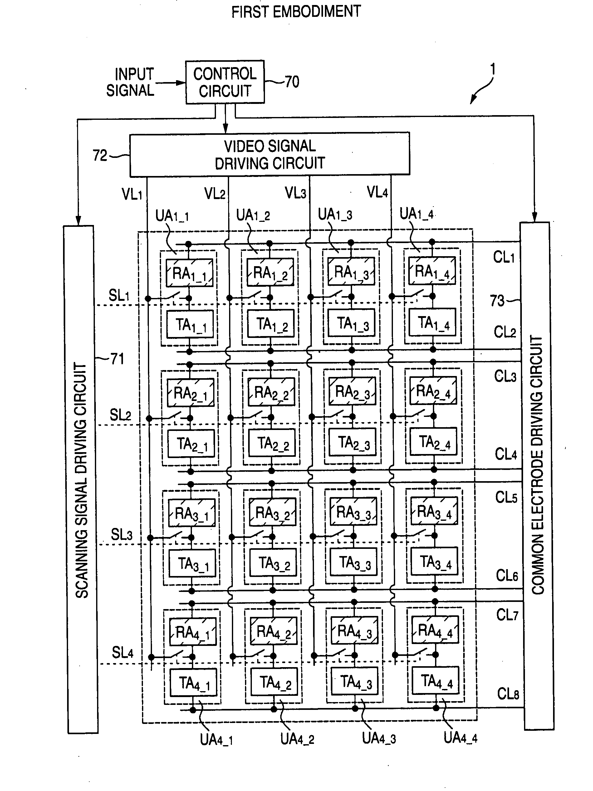
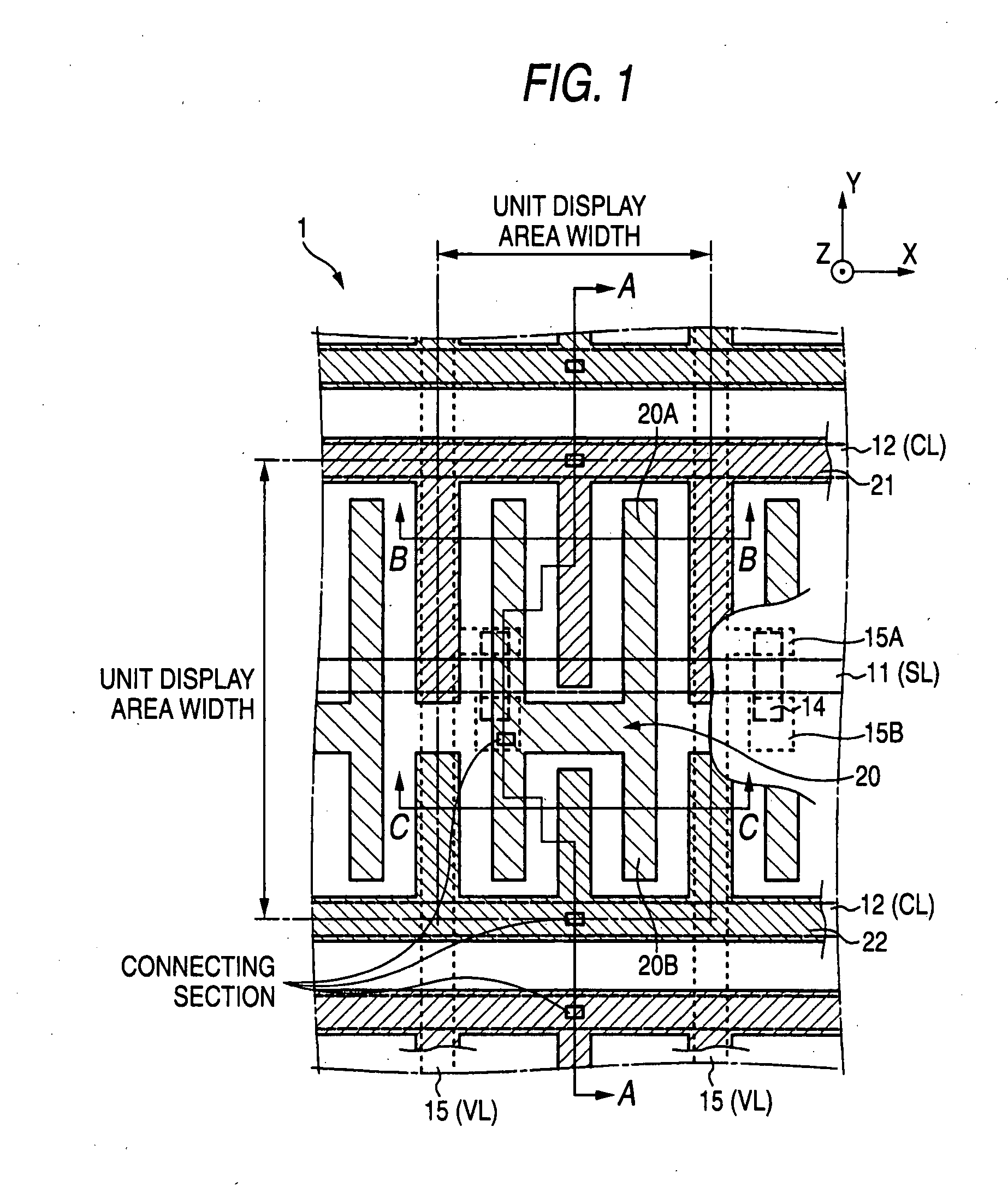
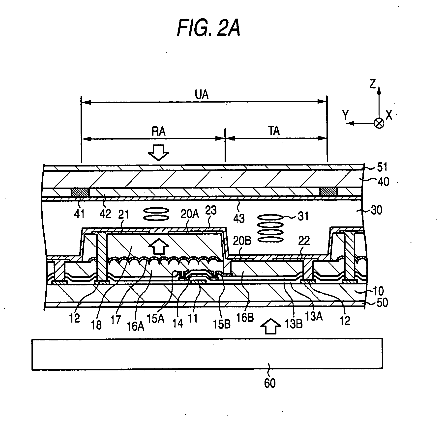
[0156]A first embodiment of the invention is directed to a liquid crystal display device. FIG. 8 is a schematic diagram of the liquid crystal display device 1 according to the first embodiment of the invention. FIG. 9 is a schematic timing chart of operations in a white display state of the liquid crystal display device 1 according to the first embodiment. FIG. 10 is a schematic timing chart of operations in a black display state of the liquid crystal display device 1 according to the first embodiment. For convenience of explanation, it is assumed that the unit display areas UA are arranged in a 4×4 matrix shape. However, an arrangement of the unit display areas UA is not limited to this. The same holds true for other embodiments described later.

[0157]For convenience of explanation, in this embodiment and the other embodiments described later, it is assumed that an absolute value of a potential difference in design between the first counter electrode 21 and the second counter electr...

Example

[0242]A second embodiment is a modification of the first embodiment. The second embodiment has a characteristic that absolute values of voltages applied to the video signal line VL and the common electrode line CL can be reduced compared with the first embodiment. The structure itself of a liquid crystal display device 2 according to the second embodiment is the same as that explained in the first embodiment. Only operations of the liquid crystal display device 2 are different from those explained in the first embodiment. Thus, the explanation of the structure of the liquid crystal display device is omitted.

[0243]In the second embodiment and embodiments described later, for convenience of explanation, only operations in a white display state are explained. FIG. 17 is a schematic timing chart of operations in a white display state of the liquid crystal display device 2 according to the second embodiment.

[0244]As in the FIG. 9 in the first embodiment, in FIG. 17, formation of an even ...

Example

Third Embodiment

[0288]A third embodiment of the invention is also directed to a liquid crystal display device. The liquid crystal display device 3 according to the third embodiment of the invention is mainly different from the liquid crystal display device 1 according to the first embodiment in that the number of common electrode lines CL is reduced.

[0289]FIG. 20 is a schematic diagram of the liquid crystal display device 3 according to the third embodiment. FIG. 21 is a schematic timing chart of operations in a white display state of the liquid crystal display device 3 according to the third embodiment.

[0290]As shown in FIG. 20, the liquid crystal display device 3 according to the third embodiment includes P (P=M+1; in the example shown in FIG. 20, P=5 because M=4) common electrode lines CL. Any one of the first counter electrode 21 and the second counter electrode 22 in each of the unit display areas UA corresponding to an m′th (m′=p−1) scanning signal line SLm′ (in the example sh...


PUM


Abstract

A semi-transmission liquid crystal display device of an in-plane switching mode includes M scanning signal lines, N video signal lines, switching elements, and a unit display area. The unit display area includes a first pixel electrode and a first counter electrode, a first storage capacitor, a second pixel electrode and a second counter electrode, and a second storage capacitor. A first voltage V1 is applied to the first counter electrode. A second voltage V2 is applied to the second counter electrode. When a higher one of the voltages V1 and V2 is represented as Hi (V1,V2) and a lower one of the voltages V1 and V2 is represented as Low (V1,V2), a third voltage equal to or lower than Hi (V1,V2) and equal to or higher than Low (V1,V2) is applied to the first pixel electrode and the second pixel electrode on the basis of an operation of the switching elements.

Description

CROSS REFERENCES TO RELATED APPLICATIONS[0001]The present invention contains subject matter related to Japanese Patent Application JP 2006-313423 filed in the Japanese Patent Office on Nov. 20, 2006, the entire contents of which being incorporated herein by reference.BACKGROUND OF THE INVENTION[0002]1. Field of the Invention[0003]The invention relates to a liquid crystal display device, and, more particularly to a semi-transmission liquid crystal display device including a reflection display area that reflects external light to display an image and a transmission display area that transmits light from a rear surface thereof to display an image. The invention also relates to an electronic apparatus incorporating such a semi-transmission liquid crystal display device.[0004]2. Description of the Related Art[0005]There is known a reflection liquid crystal display device that reflects external light with reflectors provided in pixels and does not need to include a lighting device. There ...

Claims


Application Information

Patent Timeline
IPC IPC(8): G02F1/13G09G3/36
CPCG02F1/133371G02F1/133555G02F2001/134345G09G3/3614G09G3/3655G09G2330/021G09G2300/0434G09G2300/0443G09G2300/0456G09G2300/0852G09G2320/0238G09G2300/0426G02F1/134345
Inventor WATANABE, MAKOTOSATO, TOMOHIKO
Owner JAPAN DISPLAY INC
Why Eureka
Try Eureka