Gallium Nitride Based Semiconductor Device with Reduced Stress Electron Blocking Layer

Inactive Publication Date: 2008-06-12
AVAGO TECH WIRELESS IP SINGAPORE PTE
View PDF13 Cites 46 Cited by
  • Summary
  • Abstract
  • Description
  • Claims
  • Application Information

AI Technical Summary

Benefits of technology

[0010]An illustrative embodiment of the present invention addresses the above-identified need by allowing an electron block

Problems solved by technology

Nevertheless, the implementation of conventional electron blocking layers in GaN based semiconductor lasers is problematic.
Electron blocking layers located between the MQW active layer and one of the waveguide layers have been shown to cause excessive physical str

Method used


Image

  • Gallium Nitride Based Semiconductor Device with Reduced Stress Electron Blocking Layer
  • Gallium Nitride Based Semiconductor Device with Reduced Stress Electron Blocking Layer
  • Gallium Nitride Based Semiconductor Device with Reduced Stress Electron Blocking Layer

Examples


Embodiment Construction

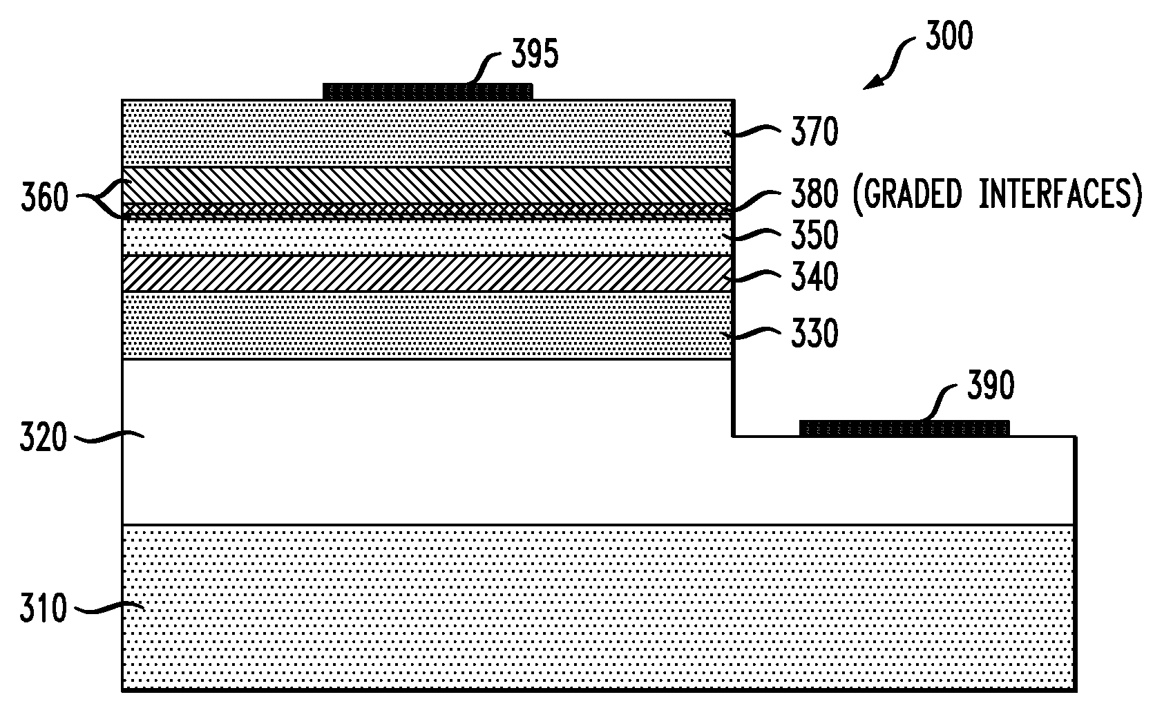
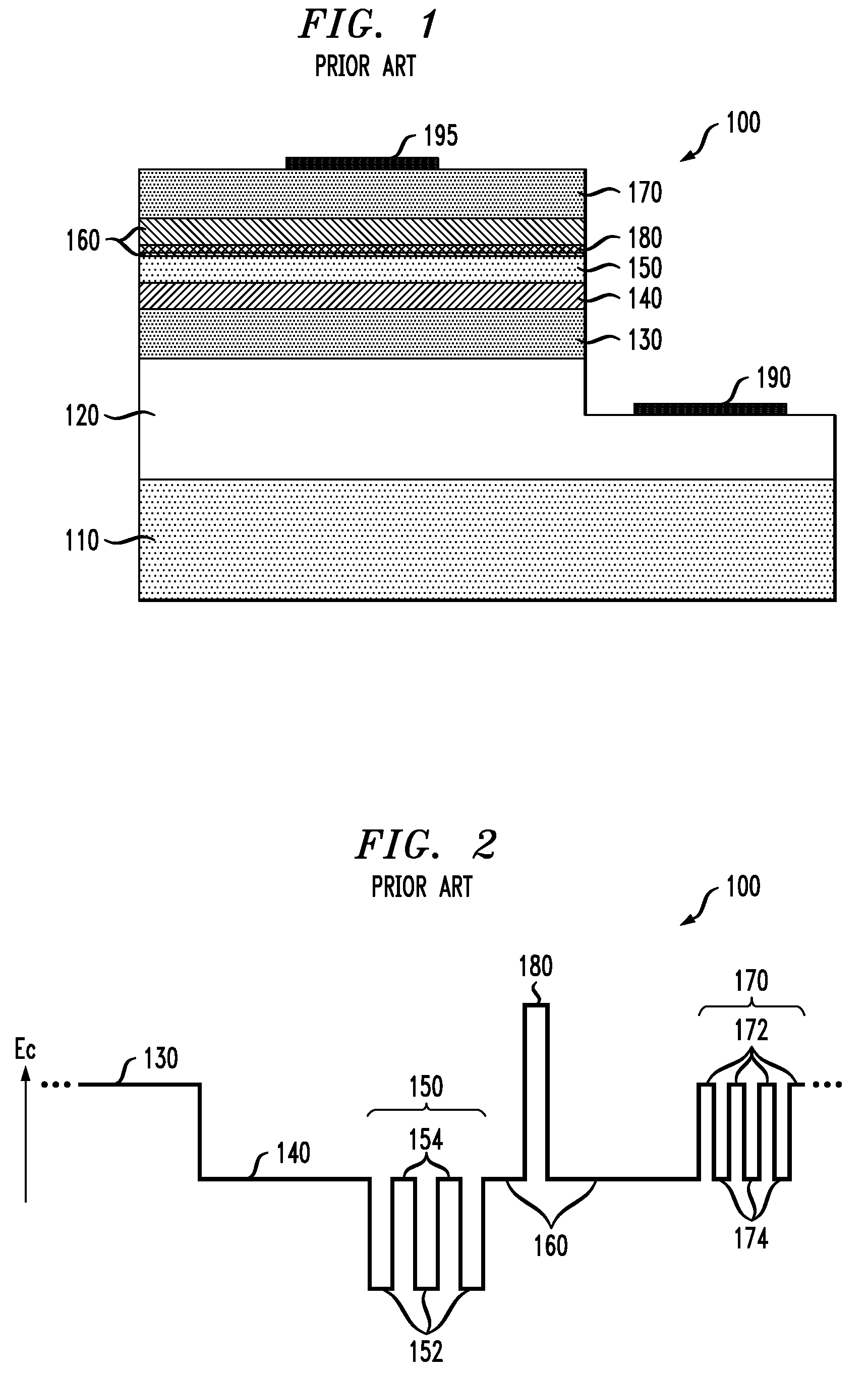
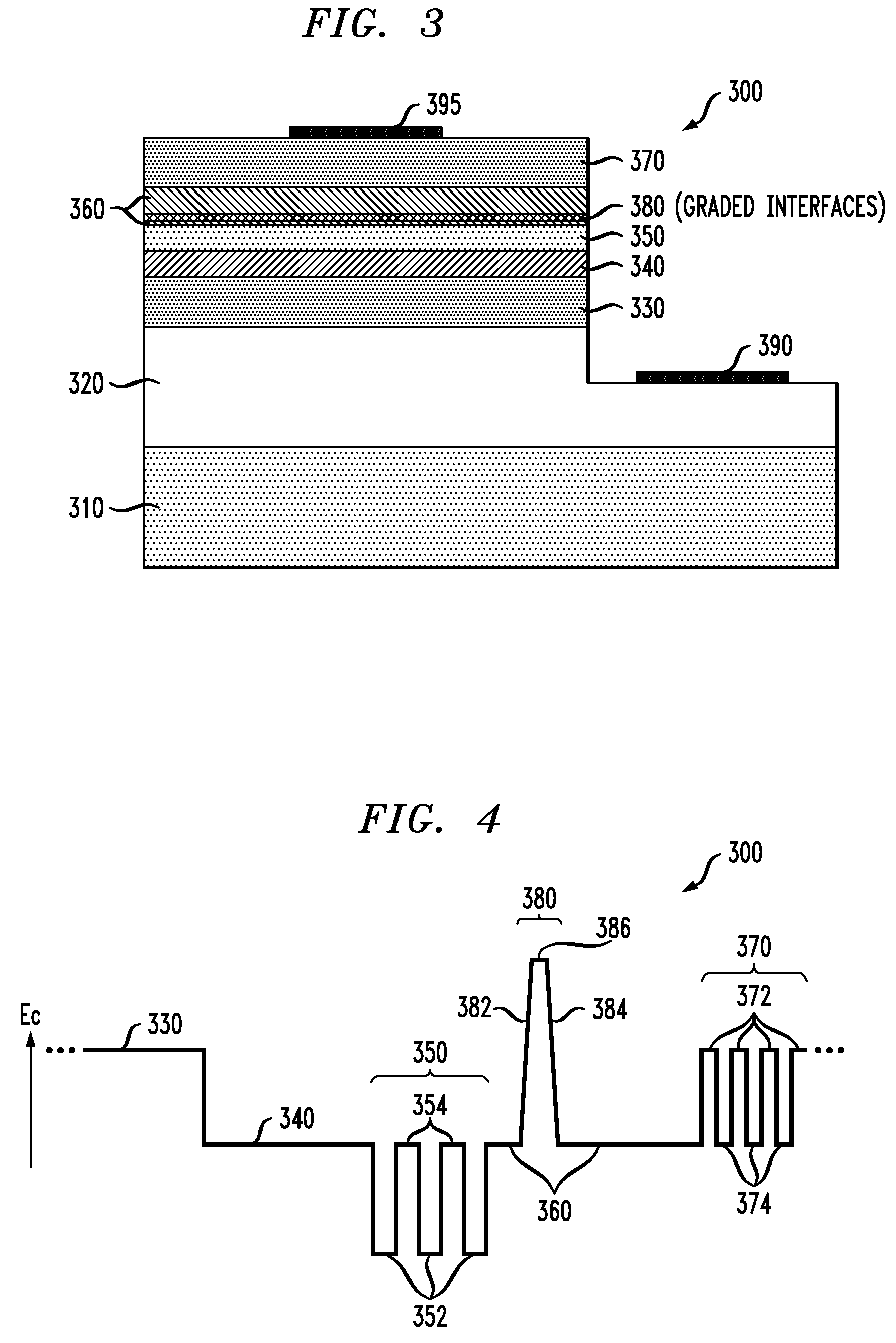
[0022]The present invention will be described with reference to illustrative embodiments in accordance with aspects of the invention. Nevertheless, the invention is not limited to these particular embodiments. Numerous modifications and variations can be made to the embodiments described herein and the results will still come within the scope of this invention. For example, while the illustrative embodiments comprise semiconductor lasers, the invention also encompasses light emitting diodes, photodetectors, optical couplers and other such semiconductor devices. Therefore, no limitations with respect to the specific embodiments described herein are intended or should be inferred.

[0023]It should be noted that the term “layer” as utilized herein is intended to encompass any stratum of matter with a given function or functions within a semiconductor device. A layer may be substantially homogenous in composition or may comprise two or more sublayers with differing compositions. For ease ...


PUM


Abstract

A semiconductor device comprises an active layer and a cladding layer. An electron blocking layer is at least partially disposed in a region between the active layer and the cladding layer and is configured to form a potential barrier to a flow of electrons from the active layer toward the cladding layer. The electron blocking layer comprises two elements from Group III of the periodic table and an element from Group V of the periodic table. One of the two elements from Group III of the periodic table has a concentration profile with a first portion that gradually increases in concentration in a direction away from the active layer toward the cladding layer and a second portion that gradually decreases in concentration between the first portion and the cladding layer.

Description

CROSS REFERENCE TO RELATED APPLICATIONS[0001]A related patent application is U.S. patent application Ser. No. 11 / 419,592, entitled “Gallium Nitride Based Semiconductor Device with Electron Blocking Layer,” which is commonly assigned herewith and incorporated by reference herein.FIELD OF THE INVENTION[0002]This invention relates generally to semiconductor devices and, more particularly, to gallium nitride (GaN) based semiconductor devices.BACKGROUND OF THE INVENTION[0003]GaN based blue-violet semiconductor lasers are likely to have far reaching technological and commercial effects. These semiconductor lasers emit near 400 nanometers, about half the wavelength of typical gallium arsenide (GaAs) based semiconductor lasers. The shorter wavelengths allow GaN based semiconductor lasers to achieve higher spatial resolution in applications such as optical storage and printing. Blu-ray DiSC™ and High Density Digital Versatile Disc (HD-DVD™) are, for example, next-generation optical disc form...

Claims


Application Information

Patent Timeline
IPC IPC(8): H01S5/323H01L33/00H01L31/0352
CPCH01S5/2009H01S5/32341H01S5/3216H01S5/3201H01S5/323H01S5/20
Inventor FREUND, JOSEPH MICHAEL
Owner AVAGO TECH WIRELESS IP SINGAPORE PTE
Why Eureka
Try Eureka