Method For Forming Dielectric Film And Method For Forming Capacitor In Semiconductor Device Using The Same

a technology of dielectric film and semiconductor device, which is applied in the direction of solid-state devices, coatings, chemical vapor deposition coatings, etc., can solve the problems of difficult to secure the dielectric capacity required for each unit cell, and deteriorating dielectric characteristic of the entire dielectric film, so as to improve the dielectric characteristic and leakage current characteristic of the capacitor used in the semiconductor devi

Inactive Publication Date: 2008-06-12
SK HYNIX INC
View PDF24 Cites 0 Cited by
  • Summary
  • Abstract
  • Description
  • Claims
  • Application Information

AI Technical Summary

Benefits of technology

[0012]In accordance with specific embodiments of the present invention, a dielectric characteristic and a leakage current characteristic of a capacitor used in a semiconductor device can be improved by forming a dielectric film using a [ZrO2]x[Al2O3]y layer, where x and y each represents 0 or a positive number. Herein, ZrO2 and Al2O3 are evenly mixed in the [ZrO2]x[Al2O3]y layer.

Problems solved by technology

Thus, it has become difficult to secure a dielectric capacity required for each unit cell.
On the contrary, the leakage current characteristic of the entire dielectric film is deteriorated due to the low band gap energy Eg of the HfO2 layer, and the dielectric characteristic of the entire dielectric film is deteriorated due to the low dielectric constant of the Al2O3 layer.
Thus, if the dielectric film is applied in a capacitor of a DRAM device, a large limitation occurs with respect to decreasing a thickness of the dielectric film.

Method used


Image

  • Method For Forming Dielectric Film And Method For Forming Capacitor In Semiconductor Device Using The Same
  • Method For Forming Dielectric Film And Method For Forming Capacitor In Semiconductor Device Using The Same
  • Method For Forming Dielectric Film And Method For Forming Capacitor In Semiconductor Device Using The Same

Examples


first embodiment

[0023

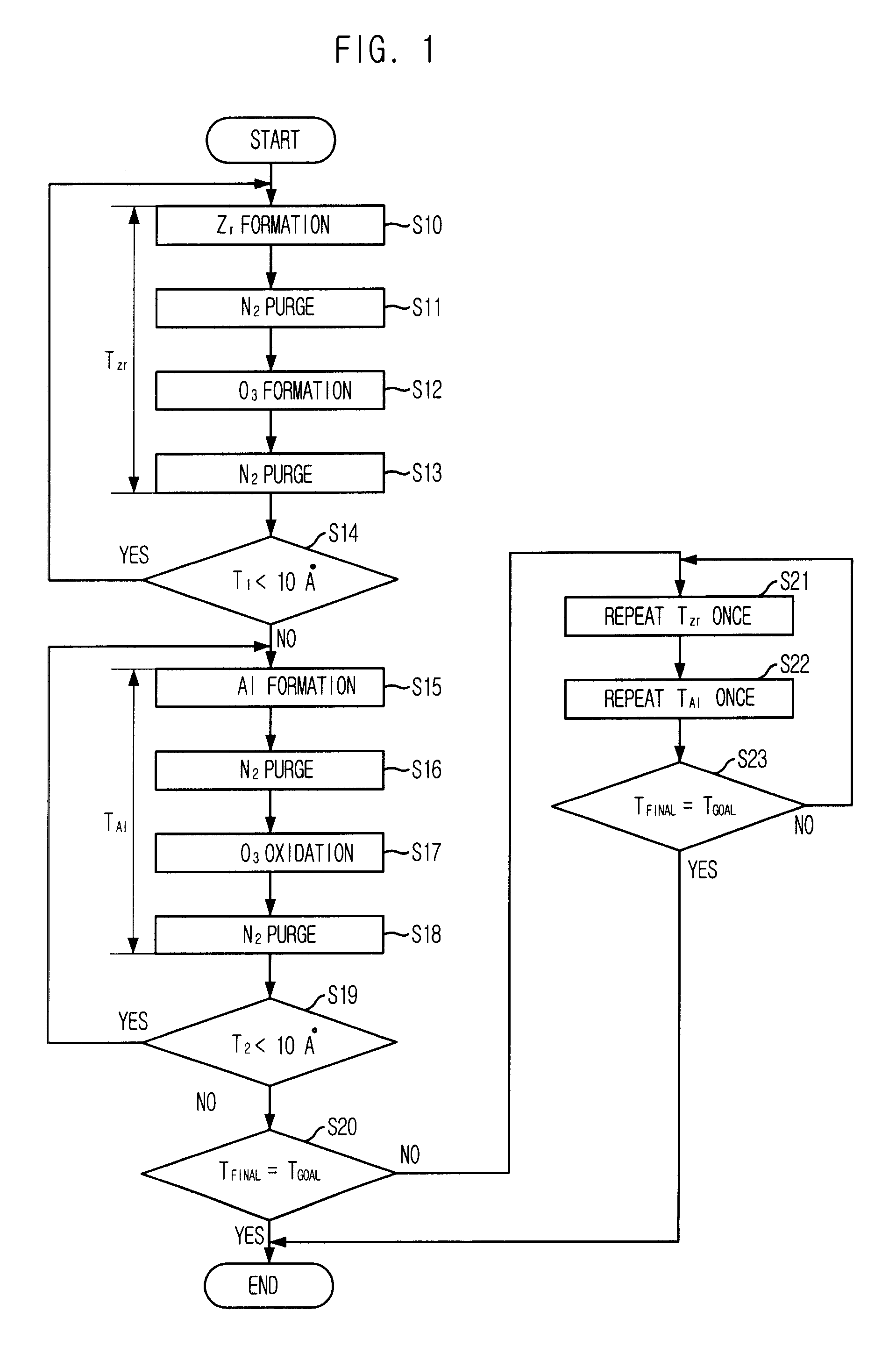
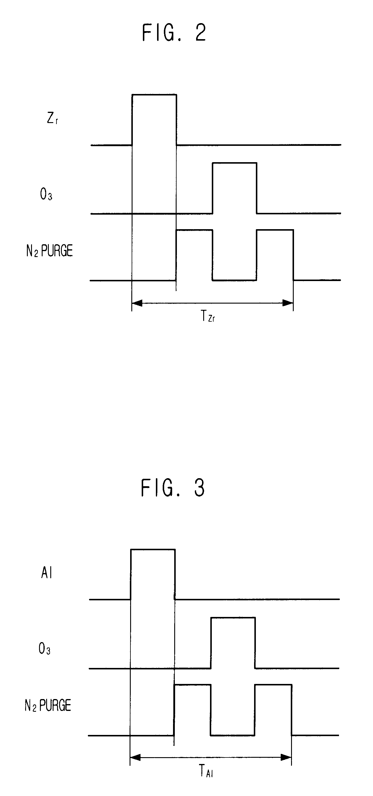
[0024]FIG. 1 is a process flowchart illustrated to describe a method for forming a dielectric film in a semiconductor device in accordance with a first embodiment of the present invention, FIG. 2 is a diagram illustrated to describe a sequential order of a zirconium dioxide (ZrO2) layer formation process, and FIG. 3 is a diagram illustrated to describe a sequential order of an aluminum oxide (Al2O3) layer formation process.

[0025]Referring to FIGS. 1 to 3, the method for forming a dielectric film in a semiconductor device in accordance with the first embodiment of the present invention includes forming a ZrO2 layer and then forming an Al2O3 layer, using an atomic layer deposition (ALD) method.

[0026]The formation process of the ZrO2 layer is as follows. One source gas selected from the group consisting of Zr(O-tBu)4, Zr[N(CH3)2]4, Zr[N(C2H5) (CH3)]4, Zr[N(C2H5)2]4, Zr(TMHD)4, Zr(OiC3H7)3(TMTD), and Zr(OtBu)4, is supplied inside a chamber of an ALD apparatus to adsorb zirconium (Z...

second embodiment

[0030

[0031]FIG. 5 is a flowchart illustrating a method for forming a dielectric film in accordance with a second embodiment of the present invention.

[0032]As shown in FIG. 5, the method for forming a dielectric film in accordance with the second embodiment of the present invention uses an ALD method like the first embodiment of the present invention. However, in the second embodiment, an Al2O3 layer is non-continuously formed over a wafer and then a ZrO2 layer is formed, instead of forming the ZrO2 layer first. Excluding such a difference, the second embodiment of the present invention is performed with substantially identical processes to the first embodiment of the present invention. Thus, detailed descriptions of the second embodiment are abridged herein for the convenience of description.

third embodiment

[0033

[0034]FIG. 6 is a flowchart illustrating a method for forming a dielectric film in accordance with a third embodiment of the present invention, and FIG. 7 is a diagram illustrating a formation process of simultaneously forming a [ZrO2]x[Al2O3]y layer.

[0035]Referring to FIGS. 6 and 7, the method for forming a dielectric film in a semiconductor device in accordance with the third embodiment of the present invention uses an ALD method to simultaneously form the [ZrO2]x[Al2O3]y layer.

[0036]A source gas such as ZrAl(MMP)2(OiPr)5, where Zr and Al are formed as one molecule, is supplied inside a chamber of an ALD apparatus to adsorb Zr and Al over a wafer, although it is not shown, at step S210. Herein, a temperature ranging from approximately 200° C. to approximately 350° C. is maintained inside the chamber. Subsequently, N2 gas is supplied inside the chamber to purge the remaining source gas, which did not become adsorbed, out of the chamber at step S211. Next, O3 is supplied inside...


PUM

PropertyMeasurementUnit
temperatureaaaaaaaaaa

Abstract

Provided is a method for forming a dielectric film in a semiconductor device, wherein the method can improve a dielectric characteristic and a leakage current characteristic. According to specific embodiments of the present invention, the method for forming a dielectric film includes: forming a zirconium dioxide (ZrO2) layer over a wafer in a predetermined thickness that does not allow continuous formation of the ZrO2 layer; and forming an aluminum oxide (Al2O3) layer over portions of the wafer where the ZrO2 layer is not formed, in a predetermined thickness that does not allow continuous formation of the Al2O3 layer

Description

TECHNICAL FIELD[0001]The present invention relates to a method for forming a dielectric film in a semiconductor device and a method for forming a capacitor using the same; and, more particularly, to a method for forming a dielectric film in a semiconductor device using an atomic layer deposition (ALD) method and a method for forming a capacitor using the same.BACKGROUND ART[0002]Recently, as the design rule of a dynamic random access memory (DRAM) has decreased, a cell region has decreased and an aspect ratio of a storage node in a capacitor has increased greatly. Thus, it has become difficult to secure a dielectric capacity required for each unit cell.[0003]Conventionally, a dielectric film has been formed in oxide / nitride / oxide (ONO) layer structure to secure a dielectric capacity. However, recent researches on forming a dielectric film with an aluminum oxide (Al2O3) layer (ε=9), a hafnium dioxide (HfO2) layer (ε=25), or a stacked layer of HfO2 / Al2O3, wherein the Al2O3 layer and t...

Claims


Application Information

Patent Timeline
Patent Type & Authority Applications(United States)
IPC IPC(8): B05D5/12
CPCC23C16/40C23C16/45529C23C16/45531H01L21/02178H01L21/02189H01L28/40H01L21/0228H01L21/3141H01L21/31616H01L21/31641H01L27/10814H01L21/02194H10B12/315C23C16/18H10B12/00
Inventor KIL, DEOK-SINHONG, KWONYEOM, SEUNG-JIN
Owner SK HYNIX INC
Why Eureka
Try Eureka