Layout data generation equipment of semiconductor integrated circuit, data generation method and manufacturing method of semiconductor device

a technology of integrated circuits and data generation equipment, applied in cad circuit design, program control, instruments, etc., can solve the problems of increased resistance of wires, reduced cross-section area of metal wires, and loss of electrical conduction of wires

Inactive Publication Date: 2008-06-12
KK TOSHIBA
View PDF5 Cites 12 Cited by
  • Summary
  • Abstract
  • Description
  • Claims
  • Application Information

AI Technical Summary

Benefits of technology

[0011]According to one embodiment of the present invention, a layout data generation equipment for a semiconductor integrated circuit comprises a logic circuit designing section which designs a logic circuit based on information of the specifications of a semiconductor integrated circuit, a layout data generation section which creates layout data based on said logic circuit, a resistance information extraction section which extracts resistance information of a wire from said layout data, a circuit simulation execution section which executes a circuit simulation, an identification section of current direction which identifies a direction of a current in said wire based on said resistance information of a wire and an execution result of said circuit simulation, a verification section which verifies whether layout data of said wire breaks a design rule, said design rule being extracted from said information of the specifications of a semiconductor integrated circuit, based on a current direction of said wire and said verification section generates this verification result, and a data output section which outputs said layout data which is generated by said layout data generation section and said verification section verifies all of said wires do not break said design rule.
[0012]According to one embodiment of the present invention, a manufacturing method of layout data of a semiconductor integrated circuit comprises designing a logic circuit based on information of the specifications of a semiconductor integrated circuit, generating layout data based on said logic circuit, extracting resistance information of each wire from said layout data, executing a circuit simulation based on said layout data, identifying a direction of each current which flows in each of said wires based on said resistance information of each of said wires and on an execution result of said circuit simulation, verifying whether said layout data of each of said wires breaks a design rule included in said information of the specifications of said semiconductor integrated circuit based on information of said identified direction of each current which flows in each of said wires and generating a verification result, and outputting said layout data when all of said wires are verified as not breaking said design rule.
[0013]According to one embodiment of the present invention, a manufacturing method of a semiconductor device comprises designing a logic circuit based on information of the specifications of a semiconductor integrated circuit, generating layout data based on said logic circuit, extracting resistance information of each wire from said layout data, executing a circuit simulation based on said layout data, identifying a direction of each current which flows in / to each of said wires based on said resistance information of each of said wires and on an execution result of said circuit simulation, verifying whether said layout data of each of said wires breaks a design rule included in said information of the specifications of said semiconductor integrated circuit based on information of said identified direction of each current which flows in each of said wires and generating a verification result, and forming a pattern on a substrate based on said layout data where all of said wires are verified as not breaking said design rule.

Problems solved by technology

When a sufficient number of these atom voids have accumulated, the effective cross-section area of the metal wire is reduced and finally, the wire breaks, the electrical conduction of the wire is lost, the resistance of the wire increases and failures in signal transmission may occur.
This electro-migration is becoming one of the main causes of failure in a semiconductor device.

Method used


Image

  • Layout data generation equipment of semiconductor integrated circuit, data generation method and manufacturing method of semiconductor device
  • Layout data generation equipment of semiconductor integrated circuit, data generation method and manufacturing method of semiconductor device
  • Layout data generation equipment of semiconductor integrated circuit, data generation method and manufacturing method of semiconductor device

Examples


embodiment one

[The Circumstances Related to this Invention]

[0023]The present embodiment of this invention will be explained in detail below while referring to the drawings. First, the circumstances related to the present invention will be explained below using the drawings.

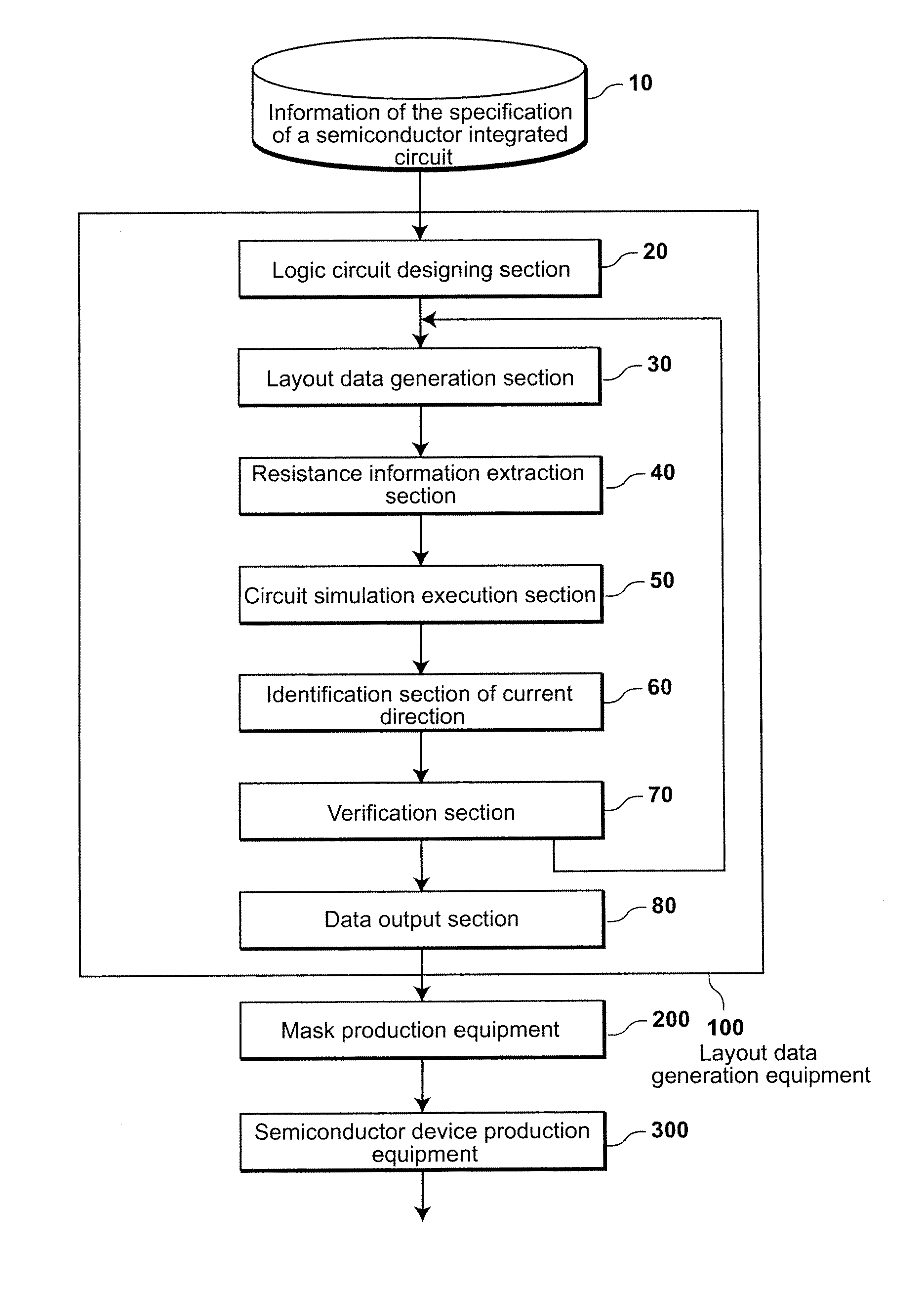
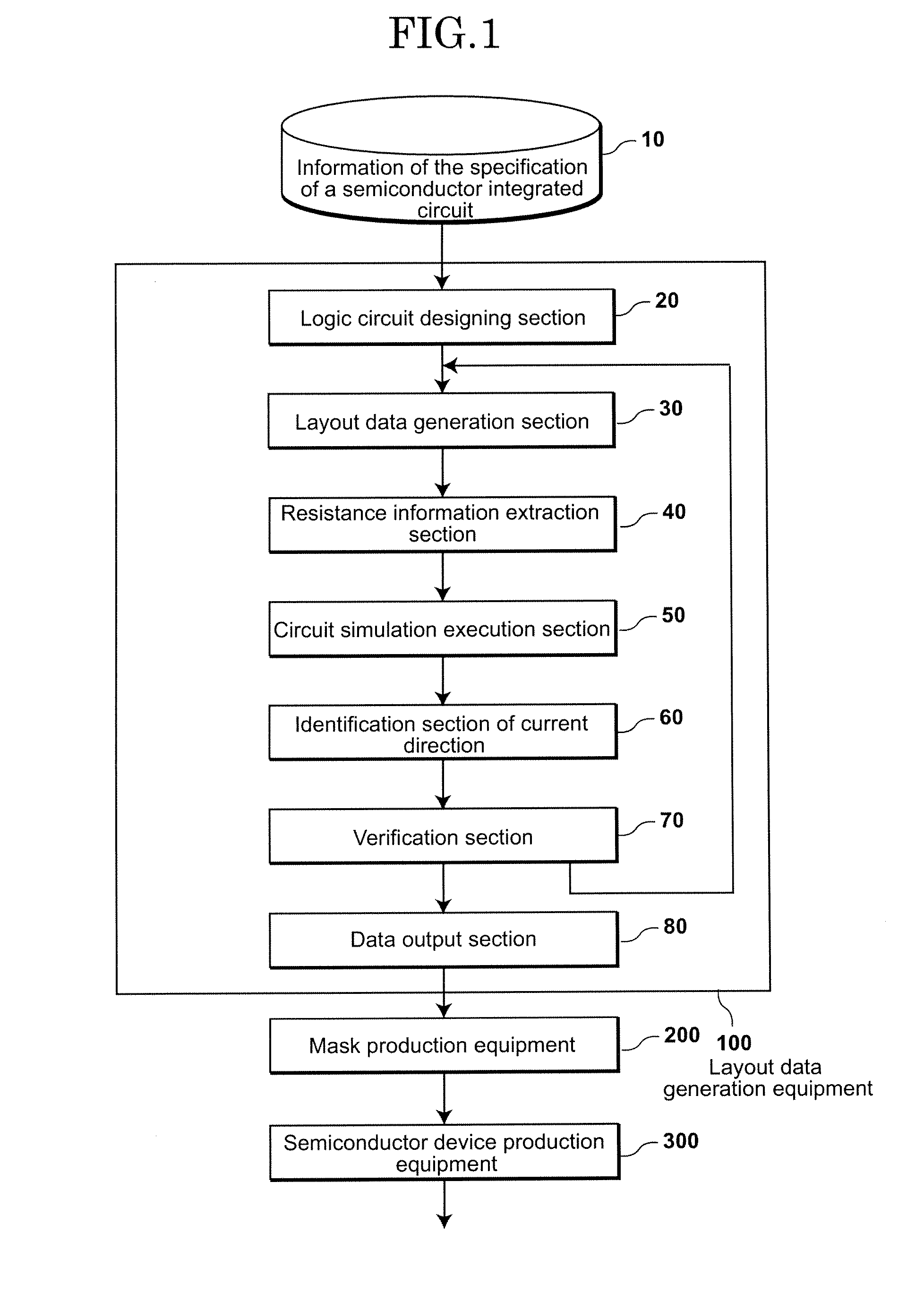
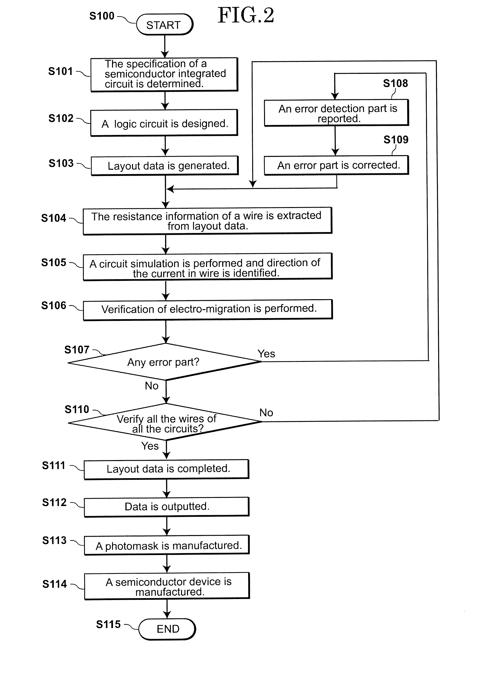
[0024]FIG. 8 is a flowchart which shows the general operation of a layout data generation method which executes a verification of electro-migration in the process which creates layout data of a semiconductor integrated circuit.

[0025]As is shown in FIG. 8, first the designer decides the specifications of a semiconductor integrated circuit (step S1001). Next, the designer designs a logic circuit based on information of these specifications (step S1002). Next, the designer creates layout data based on the designed schematic of the logic circuit (step S1003). Next, the designer visually checks the layout data and selects layout data of a wire which has a fixed length and where the line width value is wide, from among the layout dat...

embodiment two

[0073]The layout data generation device, layout data generation method and the manufacturing method of a semiconductor device by this layout data generation equipment and layout data generation method of a semiconductor integrated circuit related to embodiment two of the present invention will be explained. In the layout data generation equipment 100 and the layout data generation method related to embodiment one stated above, a verification of electro-migration is conducted in all the wires of the semiconductor integrated circuit. In the layout data generation equipment 100 in embodiment two however, by the conditions which are given to the layout data generation equipment 100 by the designer in advance, a specific wire of the semiconductor integrated circuit is selected and a verification of electro-migration is executed.

[0074]The layout data generation equipment 100 related to embodiment two is the same as the layout data generation equipment 100 shown in FIG. 1 in embodiment one...

embodiment three

[0080]As stated above, the possibility of electro-migration occurring in a single direction current wire is high. Consequently, in the layout data generation equipment, layout data generation method and the manufacturing method of a semiconductor device by this layout data generation equipment and layout data generation method of a semiconductor integrated circuit related to embodiment three of the present invention, a verification of electro-migration is executed only on single direction current wires among the wires which form a semiconductor integrated circuit.

[0081]The layout data generation equipment 100 related to embodiment three is the same as the layout data generation equipment 100 shown in FIG. 1 in embodiment one. Therefore, in embodiment three, an explanation of the layout data generation equipment 100 will be omitted.

[0082]FIG. 7 is a flowchart which shows the flow of operations of the layout data generation equipment 100 related to embodiment three. The operations fro...


PUM


Abstract

A layout-data generation equipment includes a logic circuit designing section which designs a logic circuit based on information of the specifications of a semiconductor integrated circuit, a layout-data generation section which creates layout-data based on the logic circuit, a resistance information extraction section which extracts resistance information of a wire from the layout-data, a circuit simulation execution section which executes a circuit simulation, an identification section of current direction which identifies a direction of a current in the wire based on the resistance information of a wire and an execution result of the circuit simulation, a verification section which verifies whether layout-data of the wire breaks a design rule, the design rule being extracted from the information of the specifications of a semiconductor integrated circuit and the verification section generates this verification result, and a data output section which outputs the layout-data.

Description

CROSS REFERENCE TO RELATED APPLICATIONS[0001]This application is based upon and claims the benefit of priority from the prior Japanese Patent Application No. 2006-320746, filed on Nov. 28, 2006; the entire contents of which are incorporated herein by reference.BACKGROUND OF THE INVENTION[0002]1. Field of the Invention[0003]This invention relates to a layout data generation equipment and layout data generation method which realizes electro-migration in the process of generating layout data of a semiconductor integrated circuit. Further, this invention relates to a manufacturing method of a semiconductor device using this generated layout data.[0004]2. Description of the Related Art[0005]At the time when a large current flows through a metal wire of a semiconductor integrated circuit, a phenomenon called electro-migration, whereby a metal atom shifts, sometimes occurs.[0006]That is, at the time when a current flows through a metal wire of a semiconductor integrated circuit, metal atom...

Claims


Application Information

Patent Timeline
Patent Type & Authority Applications(United States)
IPC IPC(8): G06F17/50
CPCG06F17/5068G06F30/39
Inventor OHSHIMA, SHIGEOSUZUKI, KIMINOBUYAMADA, KAZUHIROARIZONO, TAKAMICHI
Owner KK TOSHIBA
Why Eureka
Try Eureka