Liquid crystal display and manufacturing method thereof

a technology of liquid crystal display and manufacturing method, which is applied in the direction of semiconductor devices, instruments, chemistry apparatus and processes, etc., can solve the problems of disadvantageous affect of liquid crystal display and the inability to essentially eliminate the after-image of methods, so as to improve image quality, reduce the probability of positive and negative ions appearing, and improve conductivity

Inactive Publication Date: 2008-06-19
BEIJING BOE OPTOELECTRONCIS TECH CO LTD +1
View PDF5 Cites 24 Cited by
  • Summary
  • Abstract
  • Description
  • Claims
  • Application Information

AI Technical Summary

Benefits of technology

[0018]In the embodiments of the present invention, the conductive nano-particles are introduced between the substrates of a LCD, and therefore the probability of the positive and negative ions appearing is reduced due to the improved conductivity. On the other hand, the ions accumulate on the surfaces on the substrates because an image is displayed for a long time, and the accumulated ions can rapidly move away from the substrate when the screen of the LCD is switched to a next image due to presence of the conductive nano-particles, thus after-image will not appear and the image quality is improved.
[0019]In addition, the antistatic ability of the LCD is improved by introducing conductive nano-particles between the substrates of the LCD, thus the defects resulted from the electrostatic discharge (ESD) in a manufacturing process can be efficiently reduced and the yield can be improved.

Problems solved by technology

When the static electricity generated by the ions is high enough to change the transmittance of the liquid crystal layer, the display of the LCD will be affected disadvantageously.
However, the above methods cannot essentially eliminate the after-image.

Method used


Image

  • Liquid crystal display and manufacturing method thereof
  • Liquid crystal display and manufacturing method thereof
  • Liquid crystal display and manufacturing method thereof

Examples


first embodiment

The First Embodiment

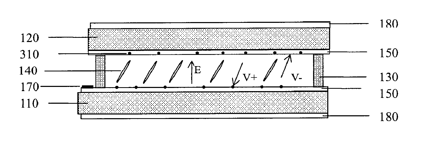
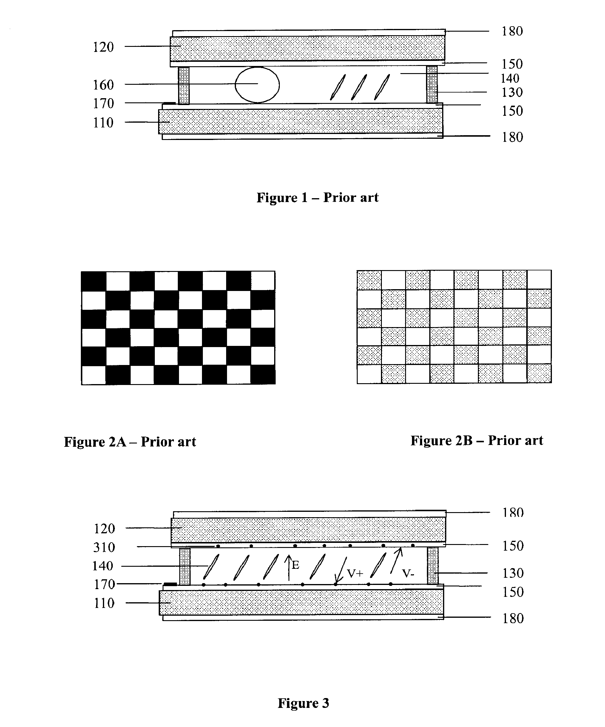
[0028]FIG. 3 is a schematic view of the structure of a LCD according to the first embodiment of the present invention, which illustrates the function of conductive nano-particles.

[0029]As shown in FIG. 3, the LCD according to the first embodiment of the present invention is a thin film transistor liquid crystal display (TFT LCD), such as a transmissive type TFT LCD. The panel of the TFT LCD comprises an array substrate 110 and a color filter substrate 120. The array substrate 110 and the color filter substrate 120 may each comprise a glass substrate and are assembled together by a sealant 130. Between the array substrate 110 and the color filter substrate 120, a dielectric anisotropic liquid crystal layer 140 is provided, one alignment layer 150 is formed on the inner surface of each of the substrates 110 and 120, and spacers 160 are disposed between the substrates 110 and 120. The spacers 160 keep a predetermined spacing between the array substrate 110 and the c...

second embodiment

The Second Embodiment

[0034]Firstly, after the formation of the array substrate 110 and the color filter substrate 120, forming the alignment layers 150 by performing a serial of processes, such as cleaning, coating material of the alignment layer, rubbing, and the like, on the inner side of each of the array substrate 110 and the color filter substrate 120. The thickness of the alignment layers is about 5 nm to about 100 nm.

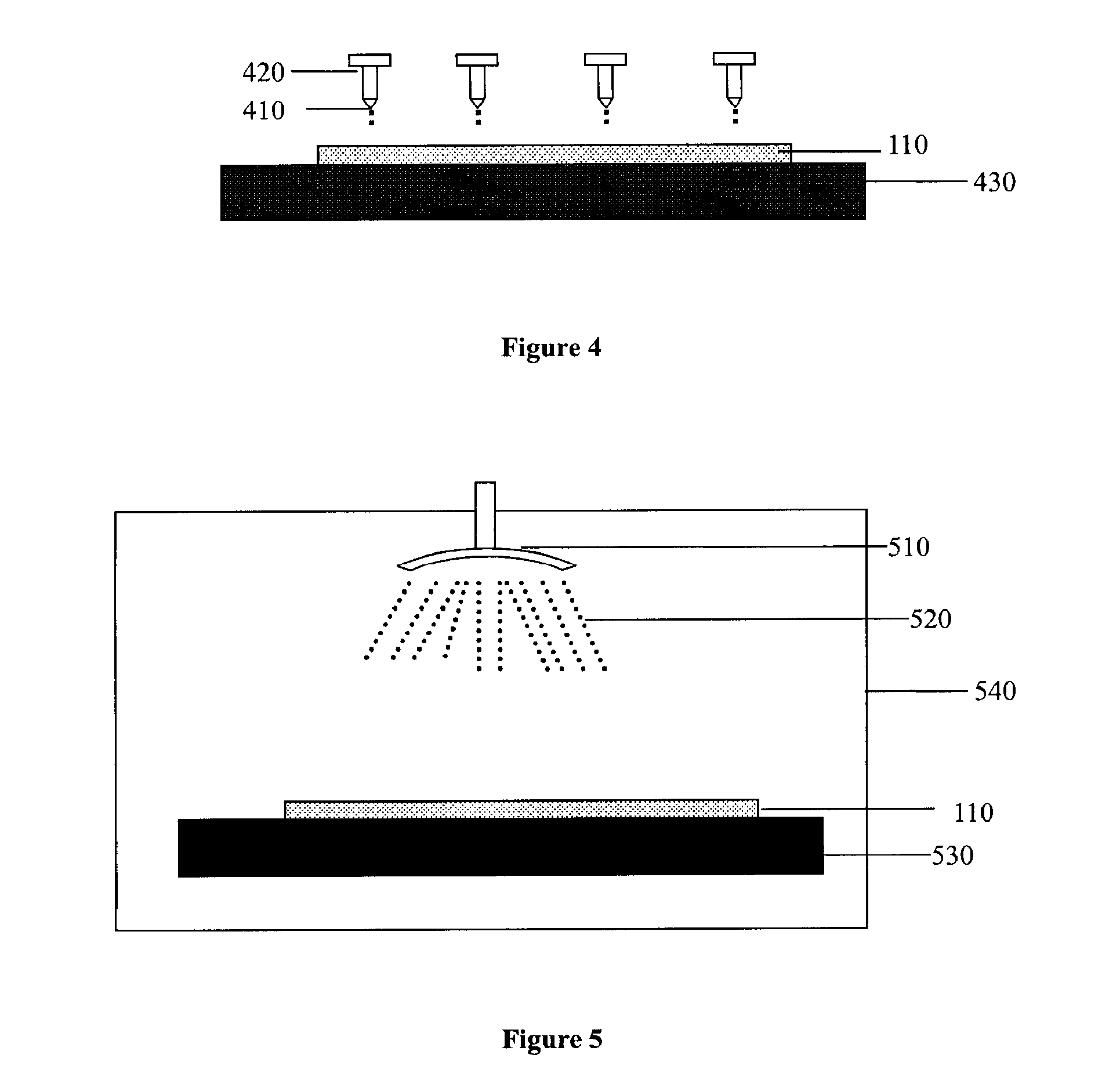
[0035]Then, after cleaning the array substrate 110 and the color filter substrate 120 formed with the alignment layers 150, a mixture solution 410 comprising the conductive nano-particles and the liquid crystal material is dispensed on the alignment layers 150 of the array substrate 110 on a base stage 430 through a nozzle 420 of a liquid crystal dispenser (not shown). The mass ratio of the conductive nano-particles to the liquid crystal ranges from about 0.01:100 to about 0.07:100. FIG. 4 is a schematic view showing dispensing the mixture solution comprising the...

third embodiment

The Third Embodiment

[0037]Firstly, after the formation of the array substrate 110 and the color filter substrate 120, forming the alignment layers 150 by performing a serial of processes, such as cleaning, coating material for the alignment layer, rubbing, and the like, on the inner side of each of the array substrate 110 and the color filter substrate 120. The thickness of the alignment layers is about 50 nm to about 100 nm.

[0038]Then, after cleaning the array substrate 110 and the color filter substrate 120 formed with the alignment layer 150, the array substrate 110 is transported to a base stage 530 of a spherical spacer spraying chamber 540, the mixture 520 of spherical spacers and the conductive nano-particles is sprayed on the surface of the alignment layer of the array substrate 110 through a nozzle of a spherical spacer spraying equipment 510. The mass ratio of the conductive nano-particles to the spherical spacers ranges from about 0.5:100 to about 3.5:100. FIG. 5 is a sch...


PUM


Abstract

A liquid crystal display (LCD) and a manufacturing method thereof. The LCD comprises a color filter substrate, an array substrate disposed opposite to the color filter substrate, and a liquid crystal layer sealed between the two substrates, wherein a conductive nano-particle is introduced between the two substrates.

Description

BACKGROUND OF THE INVENTION[0001]The present invention relates to a liquid crystal display (LCD) and a manufacturing method thereof.[0002]Among the various flat panel displays, LCDs are popularly used for the display of information processing devices, such as mobile phone, personal computer, television, and personal digital assistant (PDA), due to thin thickness, light weight, low power consumption, and low electromagnetic radiation.[0003]As shown in FIG. 1, a traditional LCD is formed by assembling an array glass substrate (TFT substrate) 110 and a color filter substrate (C / F substrate) 120, which are opposing with each other, with a sealant 130. A dielectric anisotropic liquid crystal layer 140 is disposed between the two substrates, one alignment layers 150 is provided on the inner side of each of the substrates, respectively, and a plurality of spacers 160 are formed on the surface of the substrates. When an electric field is applied between a pixel electrode on the TFT substrat...

Claims


Application Information

Patent Timeline
Patent Type & Authority Applications(United States)
IPC IPC(8): H01L33/00
CPCG02F2001/133397C09K19/52G02F1/133397
Inventor LIU, JUNGUOPARK, CHUN BAEEOM, TAE YONGZHU, HONG
Owner BEIJING BOE OPTOELECTRONCIS TECH CO LTD
Why Eureka
Try Eureka