Circuit board structure with embedded semiconductor chip

a semiconductor chip and circuit board technology, applied in the direction of semiconductor devices, semiconductor/solid-state device details, electrical equipment, etc., can solve the problems of increasing the manufacturing cost, uneven thermal stress, deteriorating electrical performance, etc., to prevent the damage of the semiconductor chip and avoid warpage of the circuit board structure

Inactive Publication Date: 2008-06-19
PHOENIX PRECISION TECH CORP
View PDF3 Cites 20 Cited by
  • Summary
  • Abstract
  • Description
  • Claims
  • Application Information

AI Technical Summary

Benefits of technology

[0013]Moreover, in the present invention, the number of the laminating layer is adjusted based on the number of the circuit build up structure, forming at least one laminating layer on the first surface of the carrier board, so as to avoid warpage of the circuit board structure.
[0014]Therefore, the circuit board structure with an embedded semiconductor chip of the present invention essentially forms a laminating

Problems solved by technology

It allows high pin counts, but creates a problem during high frequency application or high speed operations.
The problem is that the impedance tends to be large due to long lead paths, this deteriorates electrical performance.
Additionally, traditional packaging requires more connecting interfaces, which increases fabr

Method used


Image

  • Circuit board structure with embedded semiconductor chip
  • Circuit board structure with embedded semiconductor chip
  • Circuit board structure with embedded semiconductor chip

Examples


first embodiment

[0020]Referring to FIGS. 2A to 2F, which are cross-sectional diagrams illustrating a method for fabricating a circuit board structure with an embedded semiconductor chip of the present invention.

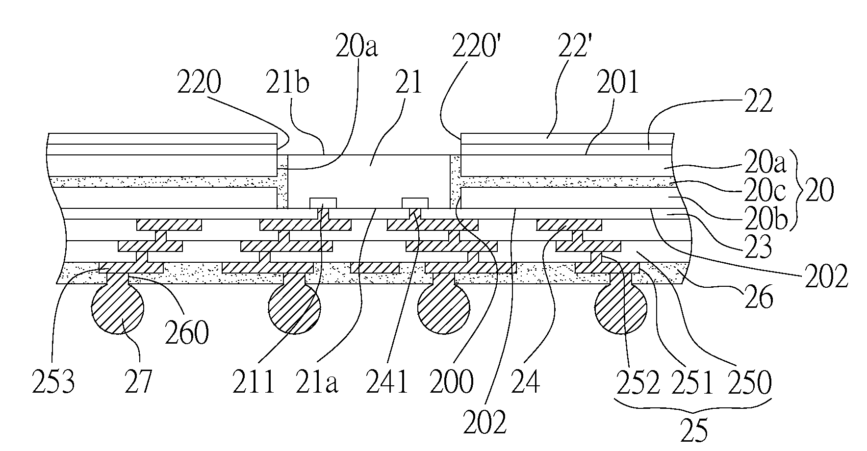
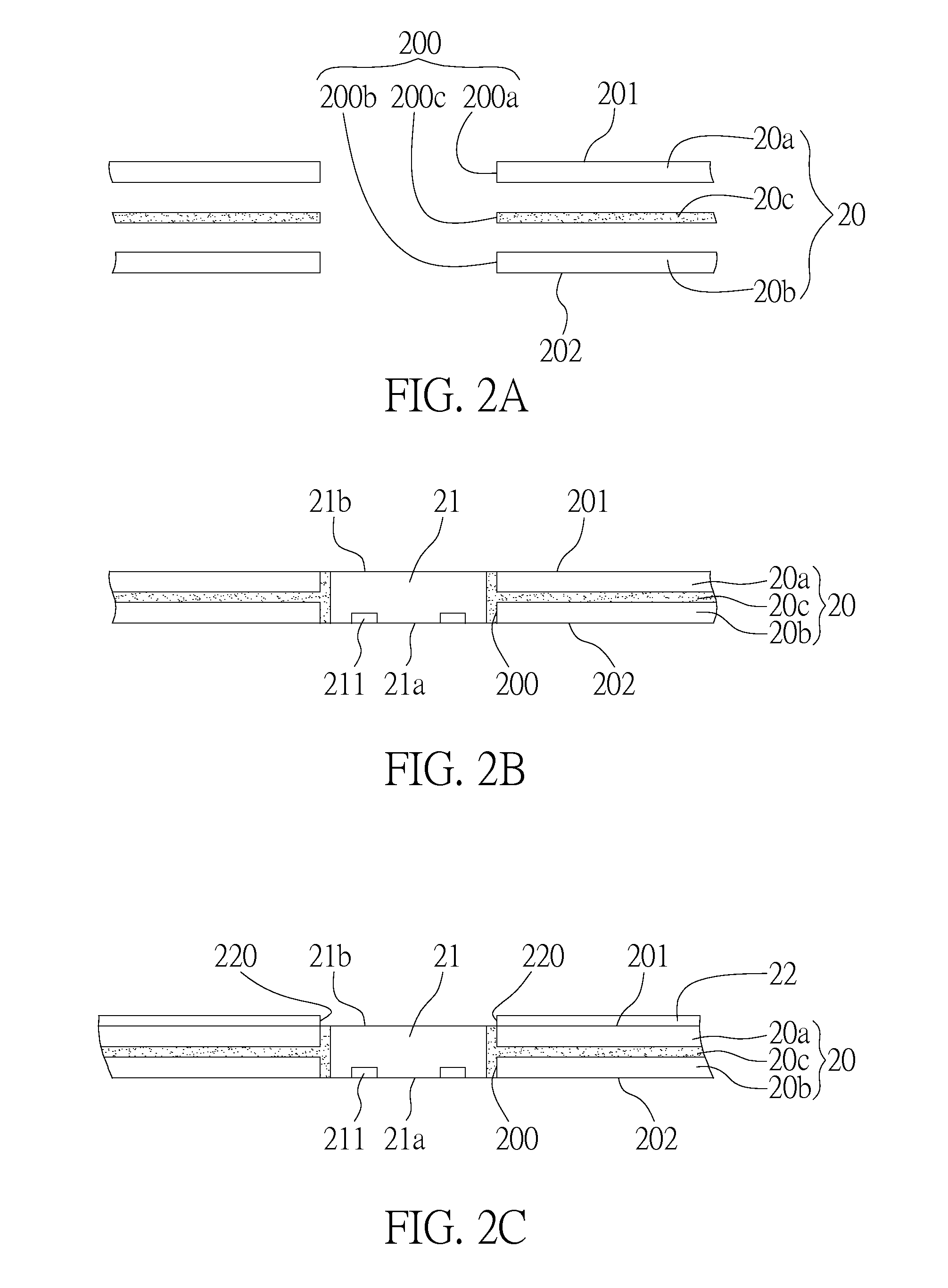
[0021]As shown in FIG. 2A, a carrier board 20 with a first surface 201 and a second surface 202 is provided. The carrier board 20 is a circuit board, insulating plate or metal plate thereon. At least two core plates 20a and 20b and an adhesive layer are provided. Through holes 200a, 200b, and 200c are formed on the core plates 20a and 20b and an adhesive layer 20c, respectively. The adhesive layer 20c is interposed between the core plates 20a and 20b, such that at least one through hole 200 is formed in the carrier board 20 penetrating through the core plates 20a and 20b and the adhesive layer 20c. The outer surfaces of the core plates 20a and 20b are the first surface 201 and the second surface 202 of the carrier board 20, respectively. The core plates 20a and 20b may be circuit boards, ins...

second embodiment

[0032]Referring to FIGS. 3A to 3D, which are cross-sectional diagrams illustrating a second embodiment of the method for fabricating a circuit board structure with an embedded semiconductor chip according to the present invention. This is different from the first embodiment in that a laminating layer is first laminated to the first surface of the carrier board before forming a dielectric layer and a circuit layer on the second surface of the carrier board.

[0033]As shown in FIG. 3A, a carrier board 20 is provided, which can be a circuit board, insulating plate or metal plate thereon; or including at least two core plates 20a and 20b and an adhesive layer 20c. Through holes 200a, 200b, and 200c are formed on the core plates 20a and 20b and an adhesive layer 20c, respectively. The adhesive layer 20c is interposed between the core plates 20a and 20b, such that at least one through hole 200 is formed in the carrier board 20 penetrating through the core plates 20a and 20b and the adhesive...


PUM


Abstract

The invention provides a printed circuit board having an embedded semiconductor chip, includes: a carrier board having a first and an opposing second surface and a through hole penetrating the first and second surfaces; a semiconductor chip disposed in the through hole and having an active surface and an inactive surface, wherein the active surface includes a plurality of electrode pads; at least one non photoimagable laminating layer formed on the first surface of the carrier board and with a through hole to expose the inactive surface of the semiconductor chip; a dielectric layer and a circuit layer formed on the second surface of the carrier board and the active surface of the semiconductor chip, wherein the circuit layer electrically connects to the electrode pads of the semiconductor chip, thereby preventing the carrier board from warpage due to temperature variations and an asymmetric structure during a single-side circuit formation process of the carrier board.

Description

FIELD OF THE INVENTION[0001]The present invention relates to a circuit board structure, and more particularly, to a circuit board structure embedded with a semiconductor chip.BACKGROUND OF THE INVENTION[0002]Various types of packaging for semiconductor devices have been developed along with the evolution of semiconductor packaging technique. Packaging mainly involves installing a semiconductor chip on a package substrate or a lead frame, then electrically connecting the semiconductor chip to the package substrate or the lead frame, and encapsulating the semiconductor chip using an encapsulation material. Ball Grid Array (BGA) is one of the advanced semiconductor packaging techniques that employs a package substrate for disposing the semiconductor chip. A plurality of solder balls in the form of grid array for connection with external devices is formed at the backside of package substrate, so as to accommodate more I / O connections on the carrier surface of the package substrate to co...

Claims


Application Information

Patent Timeline
IPC IPC(8): H01L23/48
CPCH01L23/5389H01L24/19H01L2224/04105H01L2224/20H01L2924/01033H01L2924/01082H01L2924/15311H01L2924/18162H01L2924/3011H01L2924/01029H01L2924/351H01L2924/00
Inventor HSU, SHIH-PINGCHEN, SHANG-WEI
Owner PHOENIX PRECISION TECH CORP
Why Eureka
Try Eureka