Optically compensated bend mode liquid crystal display devices and fabrication methods thereof

a liquid crystal display and bend mode technology, applied in the field of display devices, can solve the problems of complex lithographic process for limited application, and difficult to meet the requirements of forming bumps or protrusions on substrates, and achieve wide viewing angles and high-speed response time

Inactive Publication Date: 2008-06-19
IND TECH RES INST
View PDF1 Cites 9 Cited by
  • Summary
  • Abstract
  • Description
  • Claims
  • Application Information

AI Technical Summary

Benefits of technology

[0013]Embodiments of the invention provide an optically compensated bend mode liquid crystal display (OCB-LCD) device capable of achieving high-speed response time and wide viewing angles. By forming a protrusion structure and / or slit electrode structure in each pixel of the display device, multi-domains with different liquid crystal orientations are formed.

Problems solved by technology

However, for conventional LCD devices, due to a narrow viewing angle applications have been limited.
In addition, forming bumps or protrusions on substrate requires a complex lithographic process utilizing a half-tone mask.
Alignment layer formed by photo-illumination requires multiple photo-mask processes and process of placing a photo-catalyst into the alignment layer, causing fabrication complexity.
The conventional OCB-LCD device 100 however, requires adding a photo-catalyst or photo activator in the alignment layer, thus requiring expensive and intricate UV-light exposure machinery and equipment.
Moreover, multiple photo-mask processes are also required, thus further increasing production costs.

Method used


Image

  • Optically compensated bend mode liquid crystal display devices and fabrication methods thereof
  • Optically compensated bend mode liquid crystal display devices and fabrication methods thereof
  • Optically compensated bend mode liquid crystal display devices and fabrication methods thereof

Examples


Embodiment Construction

[0029]The following description is of the best-contemplated mode of carrying out the invention. This description is made for the purpose of illustrating the general principles of the invention and should not be taken in a limiting sense. The scope of the invention is best determined by reference to the appended claims.

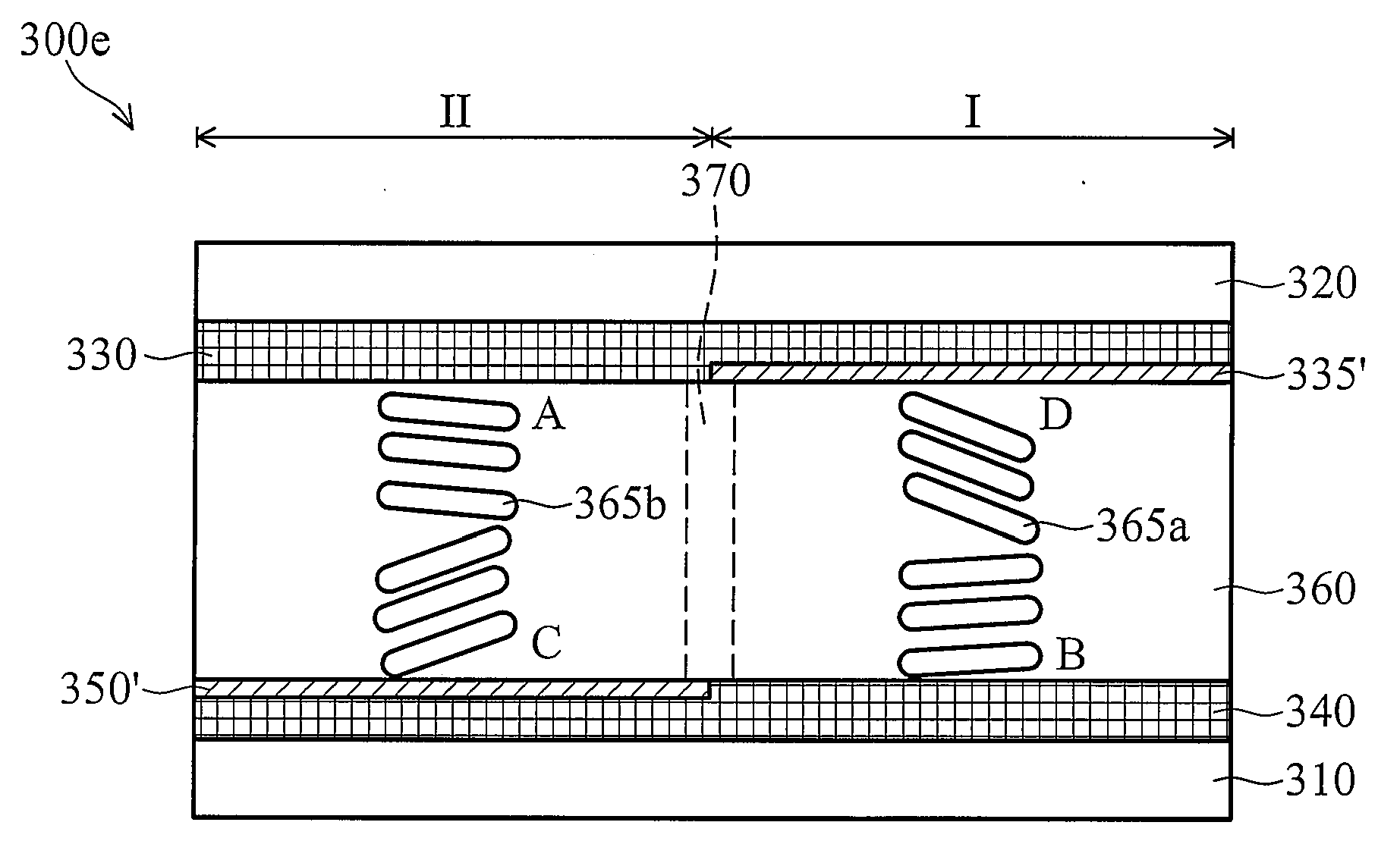
[0030]Some exemplary embodiments of the invention provide a multiple aligned domain OCB-LCD device. Applying alignment layers with different surface characteristics in each pixel regions can achieve wide viewing angles of the OCB-LCD device. Note that although some embodiments are described in conjunction with examples of an OCB mode LCD, the features of these embodiments may also be applied to other mode LCD devices with multiple aligned domains.

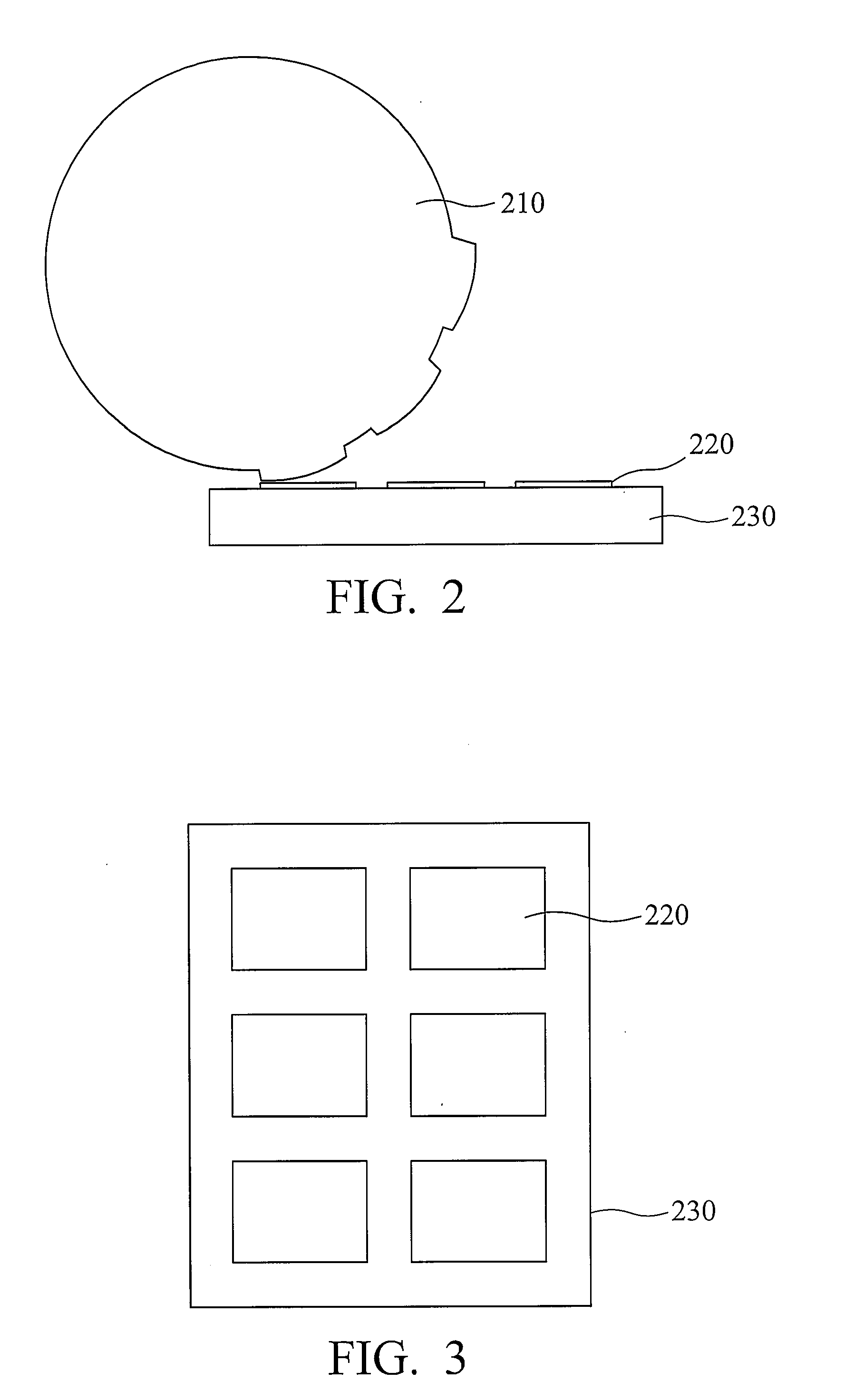
[0031]FIG. 2 is schematic view of applying an alignment layer on a substrate according to an embodiment of the invention. The alignment layer may comprise polyvinyl alcohol (PVA), polyimide (PI), polyamide (PA), polyurethane (...


PUM

PropertyMeasurementUnit
voltageaaaaaaaaaa
speedaaaaaaaaaa
volumeaaaaaaaaaa

Abstract

The invention relates to optically compensated bend (OCB) mode liquid crystal display devices and fabrication methods thereof. The OCB mode liquid crystal display includes a first substrate, a second substrate and a liquid crystal layer interposed therebetween. A first alignment layer is disposed on the first substrate, and a second alignment layer is disposed on a second region of the first substrate exposing the first alignment layer on a first region. A third alignment is disposed on the second substrate. Alignment orientations of liquid crystal molecules on the first and second alignment layers are different. When an appropriate voltage is applied to the OCB mode liquid crystal display, a splay to bend transition boundary is formed between the first and the second regions.

Description

BACKGROUND OF THE INVENTION[0001]1. Field of the Invention[0002]The invention relates to display devices, and more particularly to optically compensated bend mode liquid crystal display (OCB-LCD) devices capable of achieving high-speed response time and wide viewing angles and fabrication methods thereof.[0003]2. Description of the Related Art[0004]Liquid crystal display (LCD) devices have several advantages over other display technologies, such as a smaller volume, a lighter weight, and lower power consumption. As such, LCD devices are being applied in a variety of electronic and communication devices including notebook computers, personal digital assistants (PDA), mobile phones and others. Given the trends, technological development of LCD device are now focusing on lighter and thinner profiles with increased portability.[0005]However, for conventional LCD devices, due to a narrow viewing angle applications have been limited. To improve the viewing angle of LCD devices, multi-doma...

Claims


Application Information

Patent Timeline
Patent Type & Authority Applications(United States)
IPC IPC(8): G02F1/1337G02F1/1335H01J9/20
CPCG02F1/133753G02F1/13378G02F2001/133761G02F2001/133388G02F1/1395G02F1/133388G02F1/133761
Inventor SHA, YI-ANHSIEH, CHENG HSICHENG, WEI-YUAN
Owner IND TECH RES INST
Why Eureka
Try Eureka