Via Plating Method of System in Package and System Thereof

a technology of plating system and plating method, which is applied in the direction of electrolysis process, electrolysis components, semiconductor devices, etc., can solve the problems of difficult diffusion of cu ions to the inside of the deep via, and the plating speed is often very slow, so as to achieve the effect of effective plating layer formation and improved absorption characteristics

Inactive Publication Date: 2008-06-26
DONGBU HITEK CO LTD
View PDF8 Cites 26 Cited by
  • Summary
  • Abstract
  • Description
  • Claims
  • Application Information

AI Technical Summary

Benefits of technology

[0009]Embodiments of the present invention provide a via plating system and method. A wetting layer can be formed inside a via hole during a prepr

Problems solved by technology

However, when using Cu plating to gap-fill a deep via, it is often difficult to diffuse Cu ions to the inside

Method used


Image

  • Via Plating Method of System in Package and System Thereof
  • Via Plating Method of System in Package and System Thereof
  • Via Plating Method of System in Package and System Thereof

Examples


Embodiment Construction

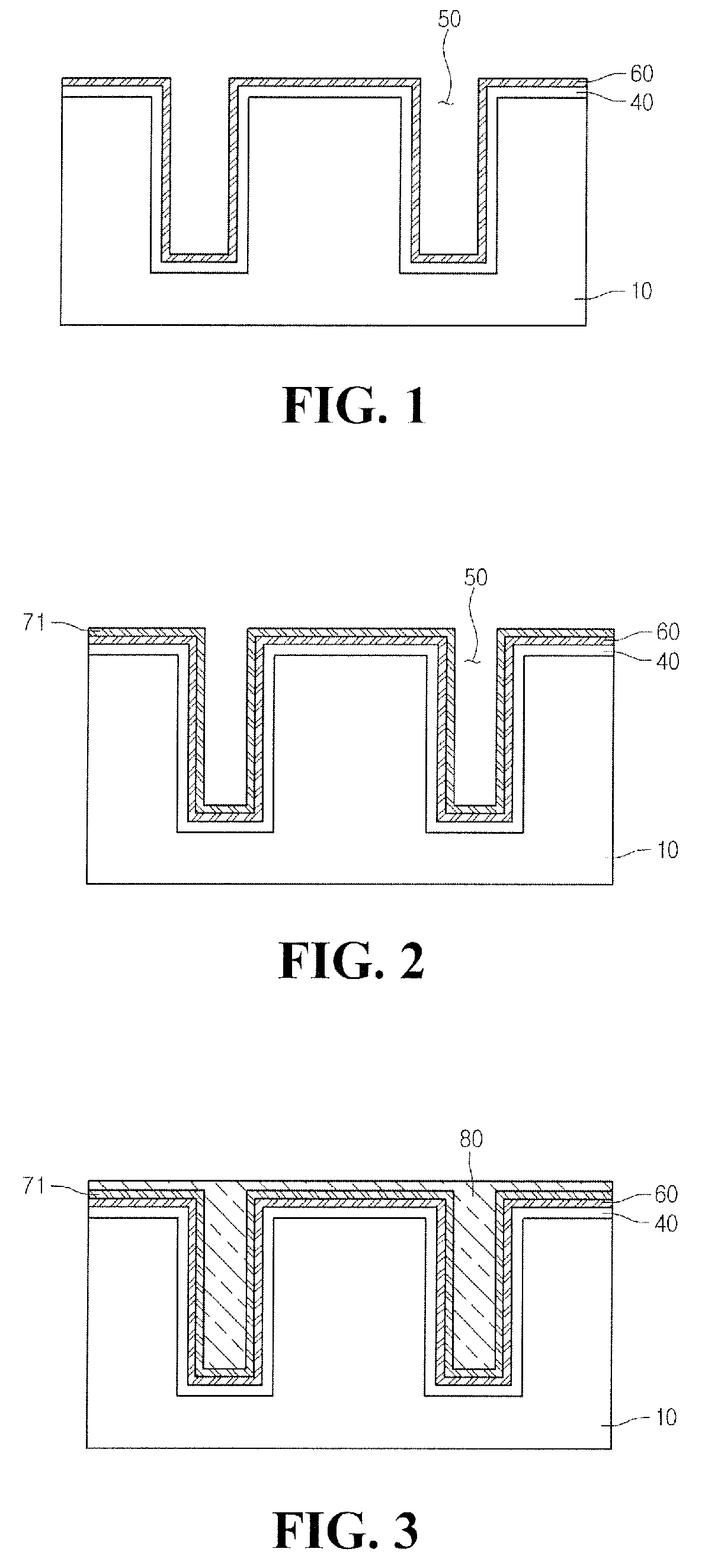
[0015]When the terms “on” or “over” are used herein, when referring to layers, regions, patterns, or structures, it is understood that the layer, region, pattern or structure can be directly on another layer or structure, or intervening layers, regions, patterns, or structures may also be present. When the terms “under” or “below” are used herein, when referring to layers, regions, patterns, or structures, it is understood that the layer, region, pattern or structure can be directly under the other layer or structure, or intervening layers, regions, patterns, or structures may also be present.

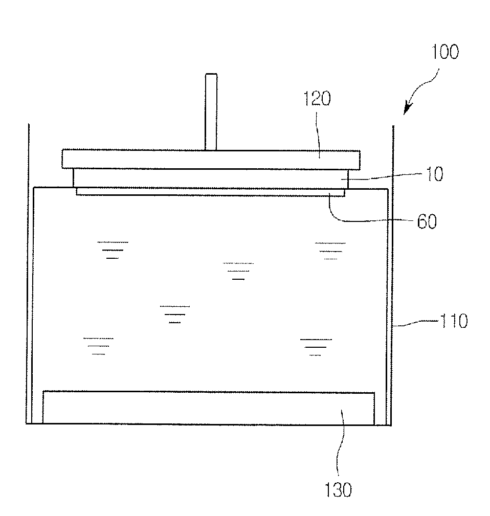
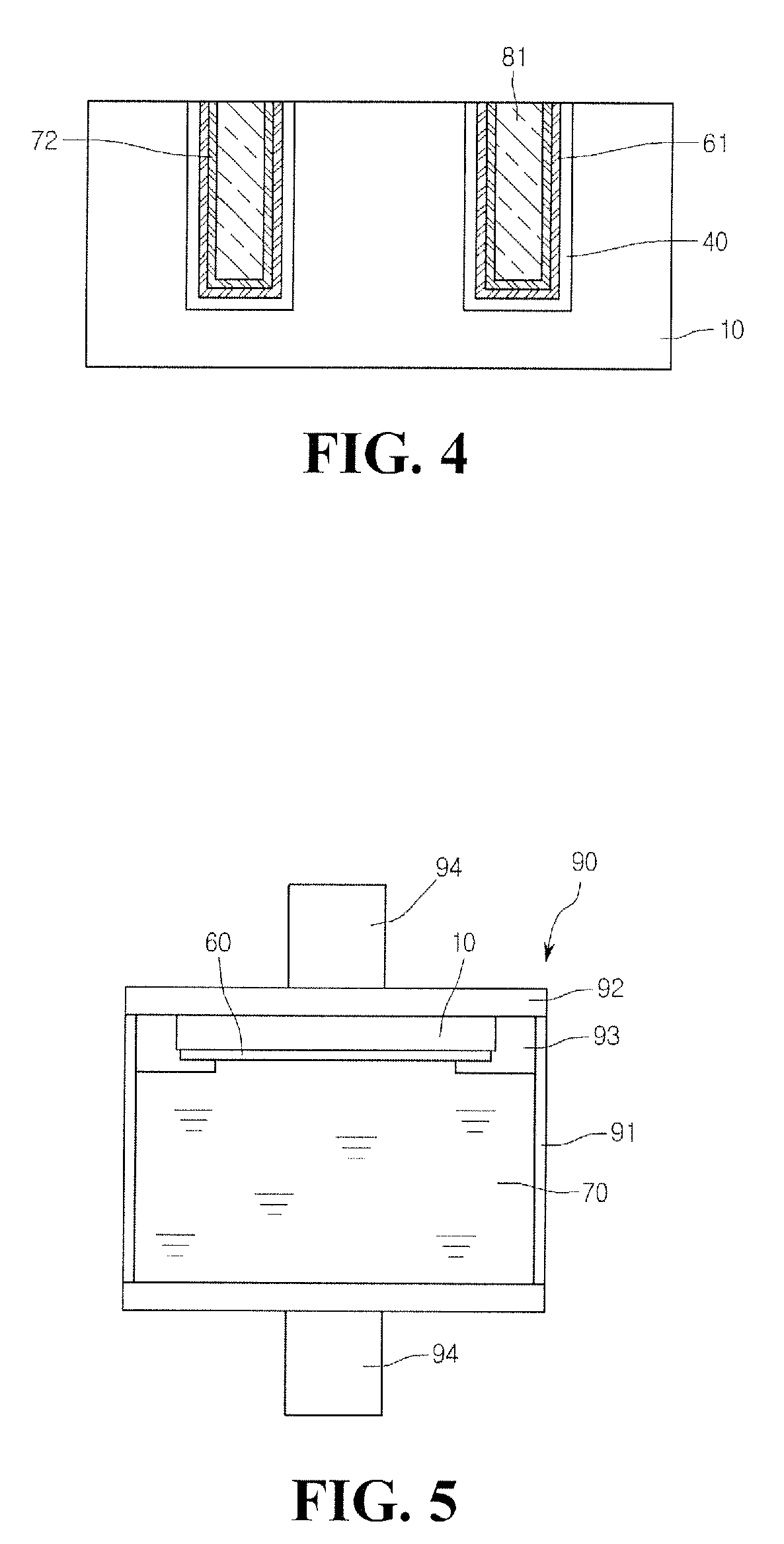
[0016]FIGS. 5 to 7 show devices used in a via plating system according to an embodiment of the present invention.

[0017]In an embodiment, the via plating system can include the use of a preprocessing device 90 (see e.g. FIGS. 5 and 6) and a plating device 100 (see e.g. FIG. 7).

[0018]Referring to FIG. 5, the preprocessing device 90 can comprise a pre-wet chamber 91, a pressing part 94, and a seal...


PUM

PropertyMeasurementUnit
Timeaaaaaaaaaa
Timeaaaaaaaaaa
Pressureaaaaaaaaaa

Abstract

A via plating system and method are provided. A preprocessing procedure is performed such that a pre-wetting solution is absorbed into a via hole, forming a wetting layer thereon. A plating process is then performed to form a plating layer inside the via hole. The preprocessing procedure to form the wetting layer improves the absorbing characteristics inside the via hole, allowing the plating layer to be more effectively formed.

Description

CROSS-REFERENCE TO RELATED APPLICATION[0001]The present application claims the benefit under 35 U.S.C. §119 of Korean Patent Application No. 10-2006-0133251, filed Dec. 23, 2006, which is hereby incorporated by reference in its entirety.BACKGROUND[0002]In order to produce complicated circuits in semiconductor devices, the technique of stacking various semiconductor chips is often used.[0003]The method of stacking various kinds of semiconductor chips in a wafer state and connecting them through a via is typically referred to as a system in package (SIP).[0004]A SIP technique generally stacks various chips vertically in order to minimize the amount of space taken up by a semiconductor device.[0005]The core technique of the SIP is the via forming method for interconnecting between the chips. In particular, in order to connect the chips, it is often required to form very deeps vias, with depths of 100 μm or more.[0006]In order to gap-fill deep vias, a copper (Cu) plating method, such as...

Claims


Application Information

Patent Timeline
IPC IPC(8): H01L21/288C25D5/02
CPCC25D5/02H01L21/2885C25D17/001C25D7/123H01L21/76898H01L21/28
Inventor LEE, MIN HYUNG
Owner DONGBU HITEK CO LTD
Why Eureka
Try Eureka