

Manufacturing method of scintillator panel, scintillator panel and vacuum evaporation apparatus
a technology of scintillator and vacuum evaporation apparatus, which is applied in the direction of conversion screens, fluorescence/phosphorescence measurement, optical radiation measurement, etc., can solve the problems of insufficient image sharpness and spatial resolution of images using such technology, and the image quality is not still in the level, so as to achieve a small deterioration of image sharpness
- Summary
- Abstract
- Description
- Claims
- Application Information
AI Technical Summary
Benefits of technology
Problems solved by technology
Method used
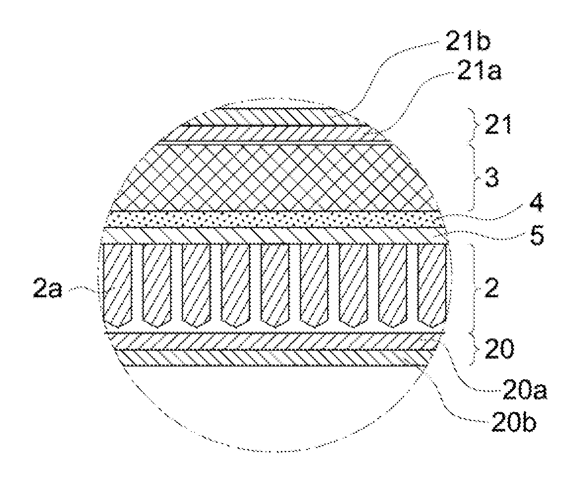
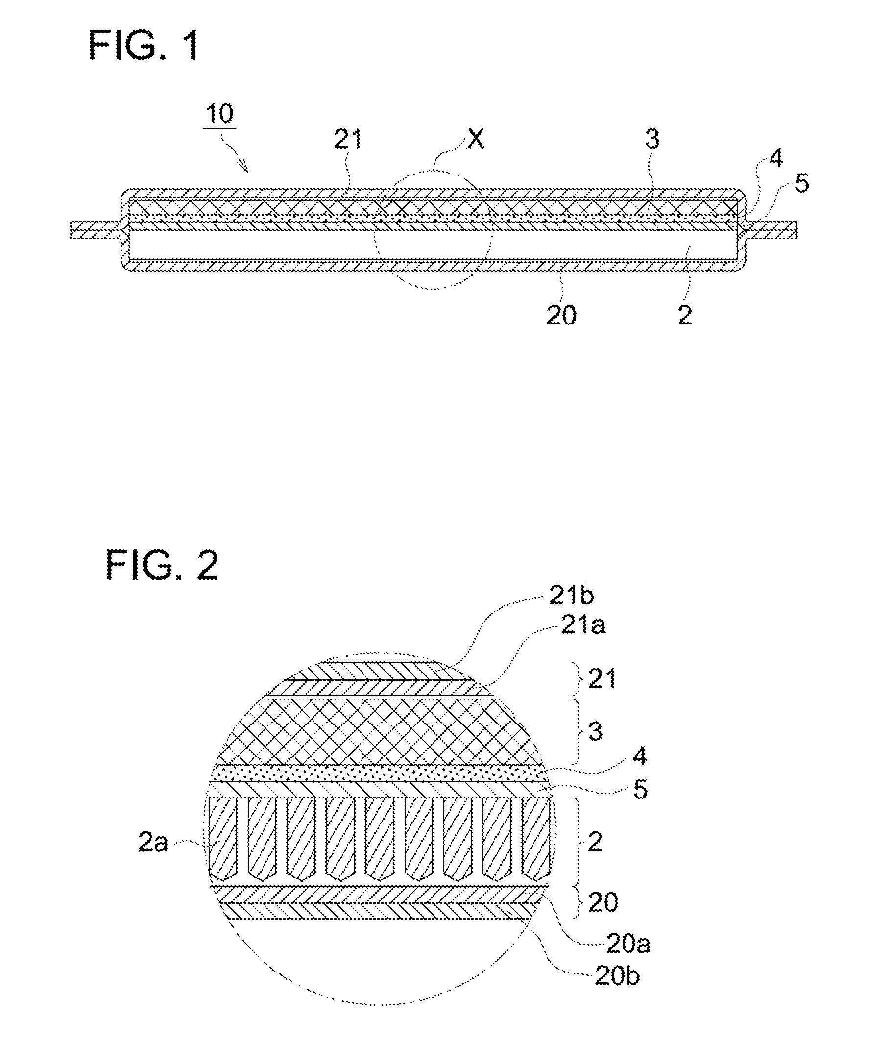
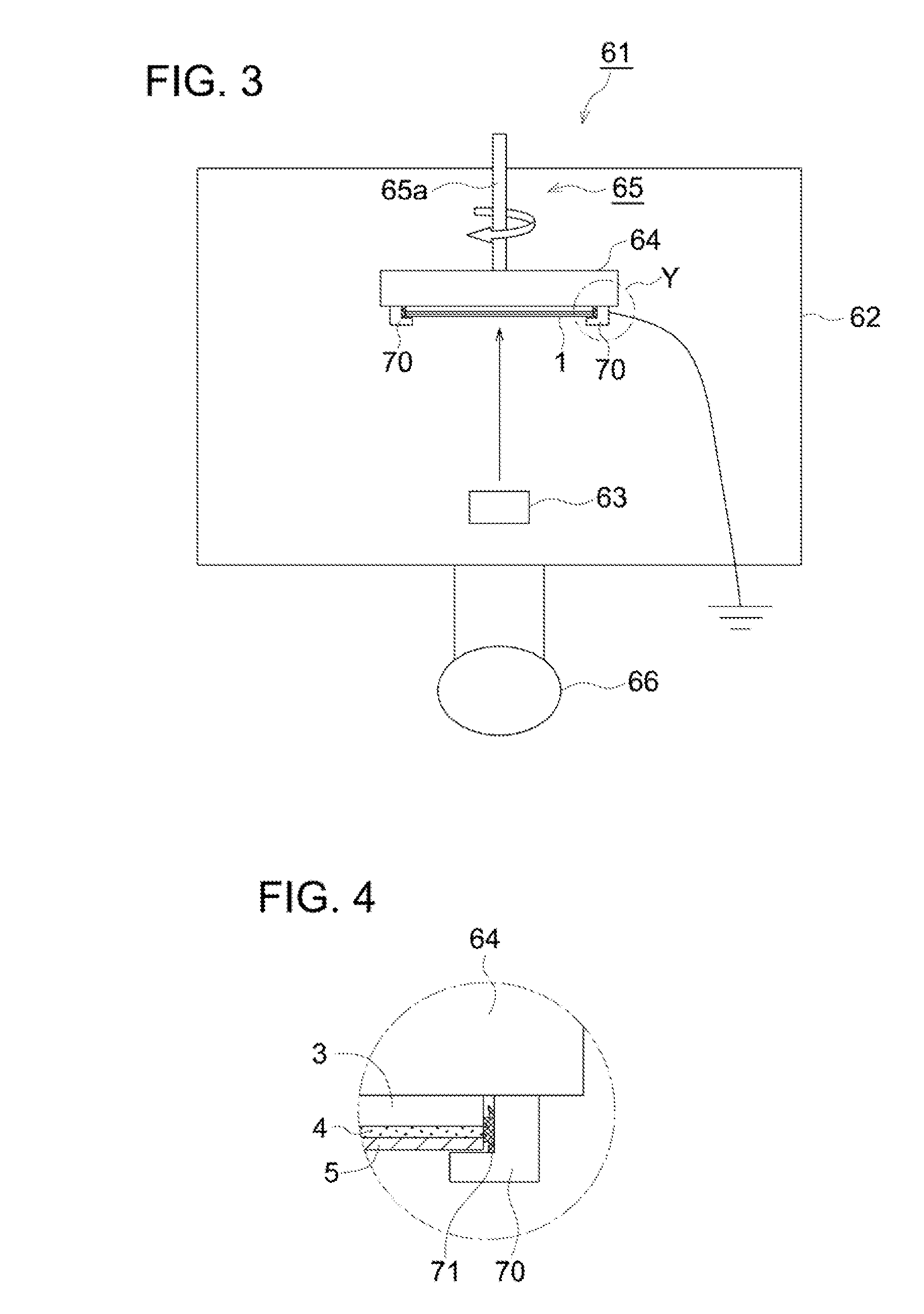
Image

Examples
example 1
Preparation of Scintillator Panel
[0117](Preparation of Substrate A Having Electroconductive Metal Reflection Layer)
[0118]Aluminum was sputtered on polyimide films (Upilex manufactured by UBE Industries Ltd.) having thicknesses of 25, 50, 75 and 125 μm to form an electroconductive metal reflection layer. Aluminum was sputtered in the same manner as above on polyimide boards having a thicknesses of 250, 500 and 750 μm each prepared by laminating the above polyimide films (Upix Board manufactured by UBE Industries Ltd.) to form an electroconductive metal reflection layer.
[0119](Preparation of Substrate B Having Electroconductive Metal Reflection Layer)
[0120]Aluminum was sputtered on polyethylene naphthalate films having thicknesses of 25, 50, 75 and 125 μm to form an electroconductive metal reflection layer.
(Preparation of protective layer)Vylon 630 (high molecular weight polyester resin100 parts by weightmanufactured by Toyobo Co., Ltd.)Methylethyl ketone (MEK)100 parts by weightTolue...
PUM
| Property | Measurement | Unit |
|---|---|---|
| thickness | aaaaa | aaaaa |
| distance | aaaaa | aaaaa |
| conductivity | aaaaa | aaaaa |
Abstract
Description
Claims
Application Information