Light emitting element housing package

a technology of light emitting elements and housing packages, which is applied in the direction of electrical equipment, semiconductor/solid-state device manufacturing, and semiconductor devices. it can solve the problems of low reliability, deterioration of efficiency in extracting light from light emitting elements, and difficulty in maintaining a white color for a long period of time. it can improve the efficiency of extracting ligh

Inactive Publication Date: 2012-03-29
TOYODA GOSEI CO LTD
View PDF1 Cites 19 Cited by
  • Summary
  • Abstract
  • Description
  • Claims
  • Application Information

AI Technical Summary

Benefits of technology

[0010]The present invention has been conceived to solve the problem and aims at providing a package for housing a light emitting element that makes it possible to enhance the efficiency for extracting light from a light emitting element without involvement of aged deterioration.

Problems solved by technology

However, a silver thin film is likely to cause a problem, like migration or oxidative corrosion, thereby raising a problem of low reliability (see Patent Document 1) and expensiveness.
Since the white resist layer is likely to undergo yellow discoloration, the layer encounters difficulty in maintaining a white color for a long period of time.
For this reason, there also arises a problem of efficiency in extracting light from a light emitting element being deteriorated with age.

Method used


Image

  • Light emitting element housing package
  • Light emitting element housing package
  • Light emitting element housing package

Examples


first embodiment

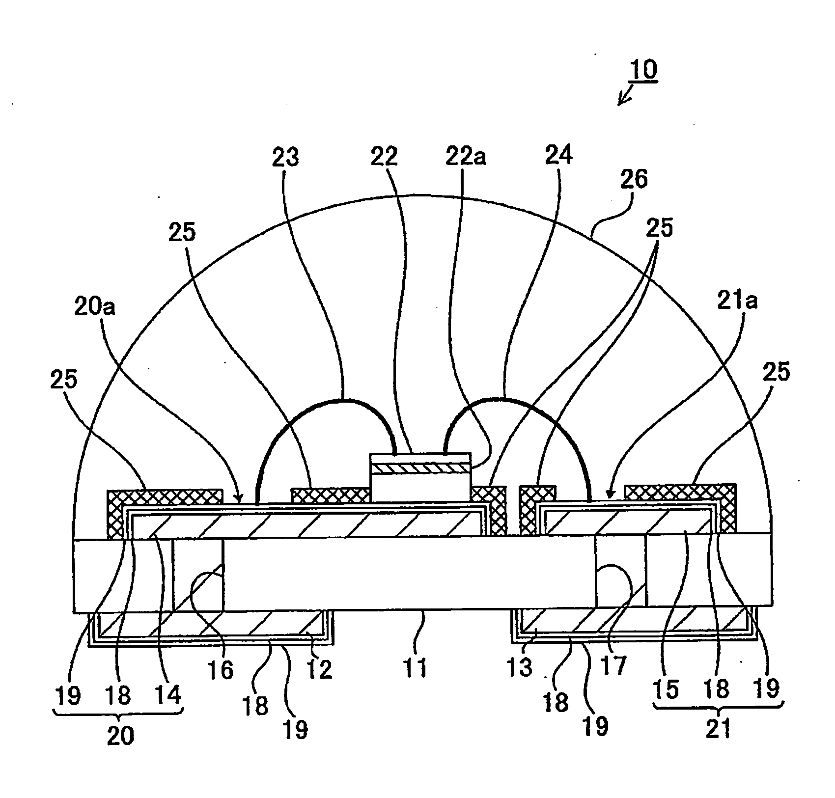
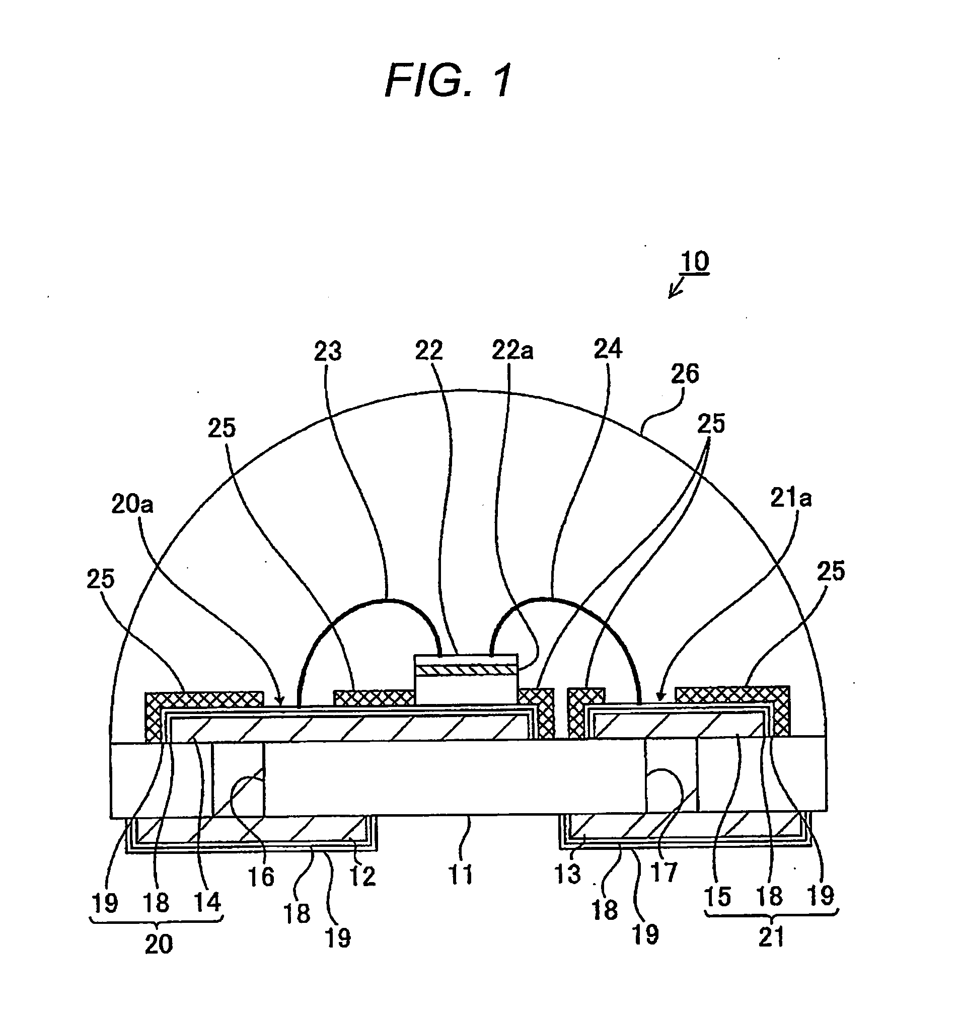
[0024]FIG. 1 is a longitudinal cross sectional view showing a general configuration of a light emitting housing package 10 of a first embodiment. The light emitting housing package 10 is made up of a ceramic substrate 11, lower electrode patterns (electrode layers) 12 and 13, upper electrode patterns 14 and 15, contact holes 16 and 17, a nickel (Ni) thin film layer 18, a gold (Au) thin film layer 19, wiring patterns (wiring layers) 20 and 21, connection regions 20a and 21a, a light emitting element chip 22, bonding wires 23 and 24, a white thin film layer 25, a translucent resin layer 26, and the like.

[0025]The plate-like ceramic substrate 11 is made of inexpensive sintered aluminum oxide (alumina ceramics).

[0026]The lower electrode patterns 12 and 13 are made of a a thick film layer of copper (Cu) and made by printing and applying Cu-containing conductor paste over a back side of the ceramic substrate 11 through use of a screen printing technique, or the like, and sintering the thu...

second embodiment

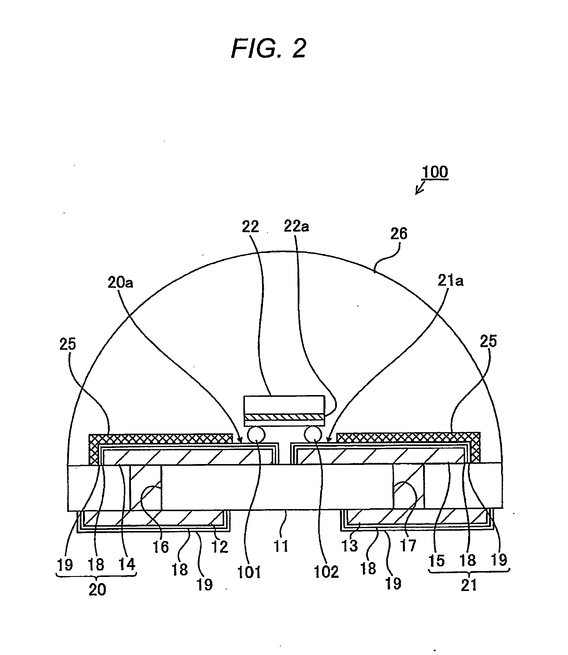
[0057]FIG. 2 is a longitudinal cross sectional view showing a general configuration of a light emitting element housing package 100 of a second embodiment.

[0058]The light emitting element housing package 100 is made up of the ceramic substrate 11, the lower electrode patterns 12 and 13, the upper electrode patterns 14 and 15, the contact holes 16 and 17, the nickel (Ni) thin film layer 18, the gold thin film layer 19, the wiring patterns 20 and 21, the connection regions 20a and 21a, the light emitting element chip 22, the white thin film layer 25, the transparent resin layer 26, bumps 101 and 102, and the like.

[0059]The light emitting element housing package 100 of the second embodiment differs from the light emitting element housing package 10 of the first embodiment in only that the light emitting chip 22 is flip-chip mounted by use of the bumps 101 and 102.

[0060]Specifically, the positive electrode of the light emitting chip 22 and the connection region 20a are electrically conn...

third embodiment

[0063]FIG. 3 is a longitudinal cross sectional view showing a general configuration of a light emitting element housing package 200 of a third embodiment.

[0064]The light emitting element housing package 200 is made up of the ceramic substrate 11, the lower electrode patterns 12 and 13, the upper electrode patterns 14 and 15, the contact holes 16 and 17, the nickel thin film layer 18, the gold thin film layer 19, the wiring patterns 20 and 21, the connection regions 20a and 21a, the light emitting element chip 22, bonding wires 23 and 24, the white thin film layer 25, the transparent resin layer 26, a reflector 201, and the like.

[0065]The light emitting element housing package 200 of the third embodiment differs from the light emitting element housing package 10 of the first embodiment in only that the reflector 201 is provided.

[0066]The reflector 201 is made of a synthetic resin, ceramics, and the like, and fixedly mounted on the front side of the ceramic substrate 11 so as to surro...


PUM

PropertyMeasurementUnit
thicknessaaaaaaaaaa
temperatureaaaaaaaaaa
reflectanceaaaaaaaaaa

Abstract

A light emitting element housing package comprises a ceramic substrate on which a light emitting element is mounted, and a wiring pattern that is formed on the ceramic substrate and to which a light emitting element chip is electrically connected, wherein a white thin film layer formed from a sintered body of white inorganic particles is formed on at least an upper surface of the wiring pattern, except a connection region in the wiring pattern to be connected to the light emitting element chip.

Description

BACKGROUND OF THE INVENTION[0001]1. Field of the Invention[0002]The present invention relates to a light emitting element housing package.[0003]2. Description of the Related Art[0004]In order to enhance efficiency in extracting light from a light emitting element, a light emitting element housing package that houses an optical semiconductor light emitting element, such as an LED, has demanded a technique for hindering a wiring pattern from absorbing light from the light emitting element.[0005]For instance, a proposed technique is for making a thin silver film exhibiting a high reflectance on a surface of a wiring pattern. However, a silver thin film is likely to cause a problem, like migration or oxidative corrosion, thereby raising a problem of low reliability (see Patent Document 1) and expensiveness.[0006]Accordingly, a technique for forming a white resist layer exhibiting high reflectance on a surface of a wiring pattern has already been proposed as described in connection with ...

Claims


Application Information

Patent Timeline
Patent Type & Authority Applications(United States)
IPC IPC(8): H01L33/60
CPCH01L33/486H01L33/60H01L2933/0091H01L2224/16225H01L2224/48227H01L2224/48091H01L2924/00014
Inventor SHIMONISHI, SHOTATAJIMA, HIROYUKITSUCHIYA, YOSUKE
Owner TOYODA GOSEI CO LTD
Why Eureka
Try Eureka