Power storage device and method for manufacturing the same

a technology of power storage and power supply, which is applied in the direction of fluid pressure measurement, liquid/fluent solid measurement, peptide measurement, etc., can solve the problems of difficult suppression of pulverization, and achieve the effect of suppressing the reduction of discharge capacity and degradation of electrolyte solution, improving cycle performance, and improving charge and discharge capacity

Inactive Publication Date: 2013-02-28
SEMICON ENERGY LAB CO LTD
View PDF0 Cites 20 Cited by
  • Summary
  • Abstract
  • Description
  • Claims
  • Application Information

AI Technical Summary

Benefits of technology

[0014]The uneven silicon layer includes a common portion covering the entire surface of the negative electrode current collector and projected portions which extend from the common portion. Since the uneven silicon layer is used in the negative electrode active material layer, the surface area of the negative electrode active material layer is large. Accordingly, in the case where the negative electrode is mounted on the power storage device, it is possible to perform charge and discharge at high speed, which enables the power storage device to have further improved charge and discharge capacity. In addition, since there is a space between the adjacent projected portions, the contact between the projected portions can be prevented even when the negative electrode active material layer is expanded due to charge, which prevents collapse and peeling of the negative electrode active material layer caused by the expansion of the projected portions. As a result, the power storage device having improved cycle performance can be manufactured.
[0015]In addition, the silicon oxide layer or the mixed layer including the silicon oxide and the silicate compound is provided over the surface of the uneven silicon layer. When the power storage device is charged, the silicon oxide layer occludes carrier ions, so that part of the silicon oxide becomes a silicate compound containing carrier ions. Therefore, in the power storage device which...

Problems solved by technology

However, in the case where silicon particles are used for a negative electrode active material, it has been difficult to suppre...

Method used


Image

  • Power storage device and method for manufacturing the same
  • Power storage device and method for manufacturing the same
  • Power storage device and method for manufacturing the same

Examples


embodiment 1

[0030]In this embodiment, the structure of a negative electrode of a power storage device having high cycle performance in which little deterioration due to charge and discharge occurs, and a method for manufacturing the negative electrode will be described with reference to FIGS. 1A to 1D and FIGS. 2A to 2C.

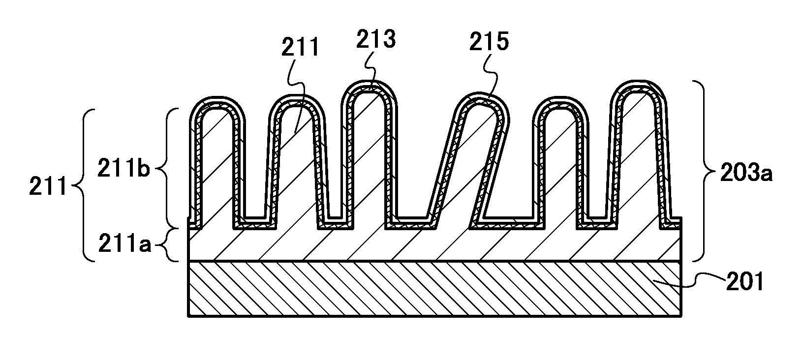
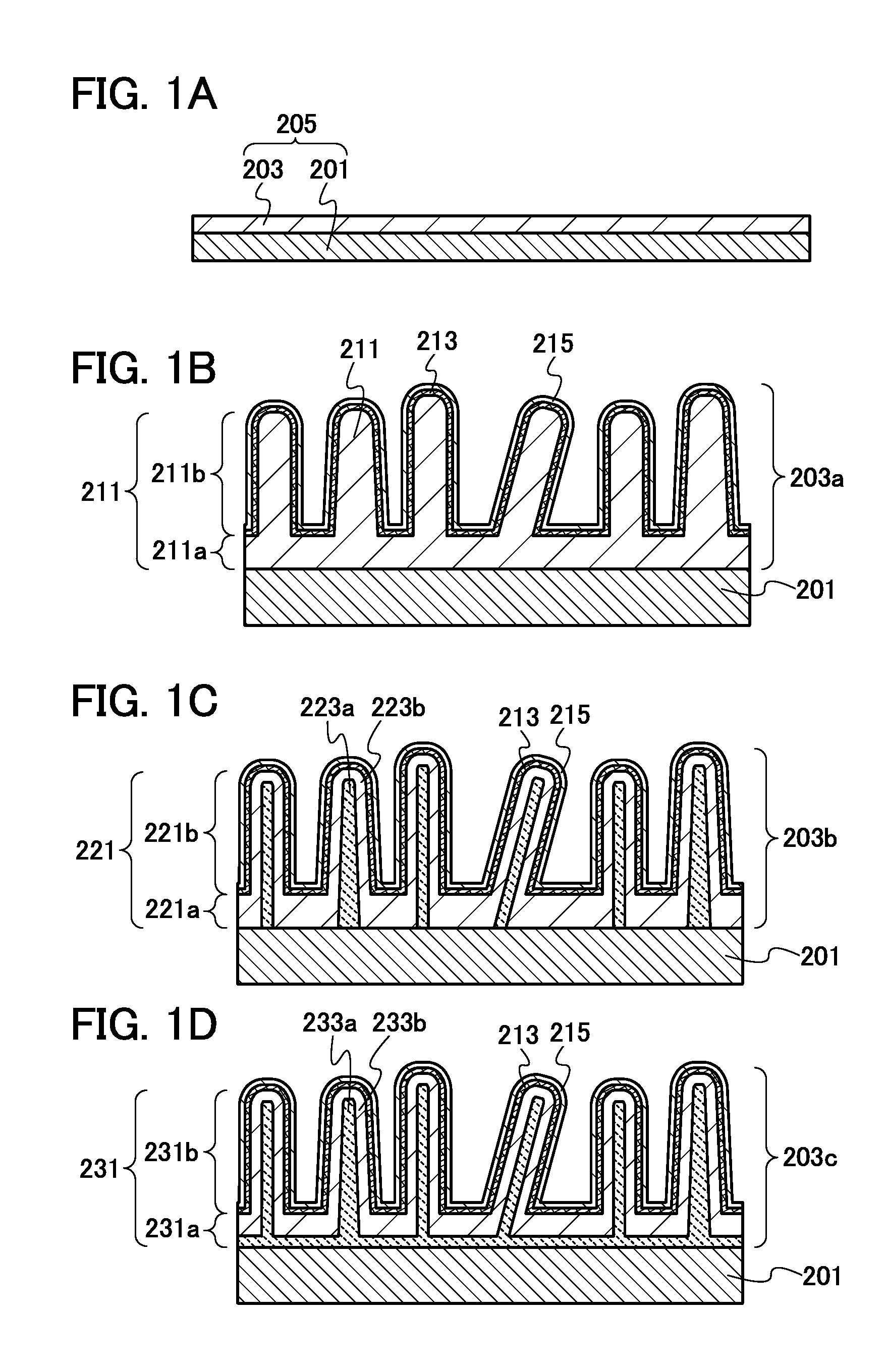
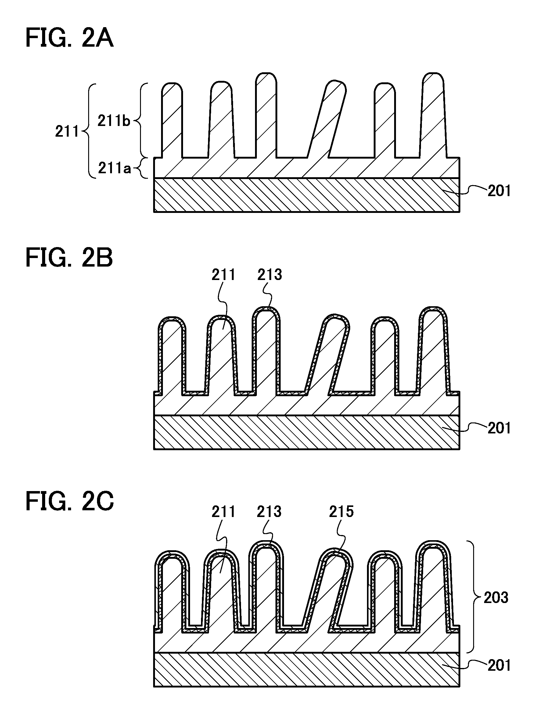
[0031]FIG. 1A is a cross-sectional view of a negative electrode 205. In the negative electrode 205, a negative electrode active material layer 203 is formed over a negative electrode current collector 201.

[0032]Note that an active material refers to a substance which relates to occlusion and release of ions serving as carriers (hereinafter referred to as carrier ions). An active material layer includes a conductive agent, a binder, a silicon oxide layer or a mixed layer described in this embodiment, graphene, or the like in addition to the active material. Therefore, the active material and the active material layer are distinguished from each other.

[0033]A secondary battery in ...

embodiment 2

[0101]In this embodiment, a method for forming the silicon oxide layer 213 which is different from the method described in Embodiment 1 will be described.

[0102]In this embodiment, the silicon oxide layer 213 can be formed by oxidation of part of the silicon layer 211. As a method for oxidizing the silicon layer 211, a method in which the silicon layer 211 is heated, a method in which the silicon layer 211 is subjected to plasma which is generated in an oxidation atmosphere, a method in which the silicon layer 211 is immersed in a solution containing oxidizer, and the like can be given.

[0103]In the method for forming the silicon oxide layer 213 over the silicon layer 211 by heating the silicon layer 211, the heating is performed at a temperature at which the silicon layer 211 is oxidized. Note that an atmosphere in the heating is preferably an oxidization gas atmosphere. Examples of an oxidization gas include oxygen, ozone, dinitrogen monoxide, and the like. Note that halogen may be ...

embodiment 3

[0107]In this embodiment, a method for forming the silicon oxide layer 213 and the graphene 215 over the silicon layer 211 which is different from the methods described in Embodiment 1 and Embodiment 2 will be described with reference to FIGS. 3A to 3C.

[0108]As illustrated in FIG. 3A, the silicon layer 211 is formed over the negative electrode current collector 201 in a manner similar to that described in Embodiment 1.

[0109]Next, the silicon layer 211 is immersed in a dispersion liquid in which graphene oxide is dispersed. Thus, as illustrated in FIG. 3B, graphene oxide 214 is attached to the silicon layer 211.

[0110]Next, heat treatment is performed at a vacuum atmosphere, a nitrogen atmosphere, or a rare gas atmosphere to reduce the graphene oxide 214, whereby the graphene 215 is formed as illustrated in FIG. 3C. In addition, in the reduction process, the silicon layer 211 and oxygen contained in the graphene oxide react with each other, whereby the silicon oxide layer 213 can be f...


PUM

PropertyMeasurementUnit
Thicknessaaaaaaaaaa
Thicknessaaaaaaaaaa

Abstract

A power storage device including a negative electrode having high cycle performance in which little deterioration due to charge and discharge occurs is manufactured. A power storage device including a positive electrode, a negative electrode, and an electrolyte provided between the positive electrode and the negative electrode is manufactured, in which the negative electrode includes a negative electrode current collector and a negative electrode active material layer, and the negative electrode active material layer includes an uneven silicon layer formed over the negative electrode current collector, a silicon oxide layer or a mixed layer which includes silicon oxide and a silicate compound and is in contact with the silicon layer, and graphene in contact with the silicon oxide layer or the mixed layer including the silicon oxide and the silicate compound.

Description

BACKGROUND OF THE INVENTION[0001]1. Field of the Invention[0002]The present invention relates to a power storage device and a method for manufacturing the power storage device.[0003]2. Description of the Related Art[0004]In recent years, power storage devices such as lithium-ion secondary batteries, lithium-ion capacitors, and air cells have been developed.[0005]An electrode for a power storage device is manufactured by forming an active material over a surface of a current collector. As the active material, a material which is capable of occluding and releasing ions serving as carriers, such as carbon or silicon, is used. For example, silicon or phosphorus-doped silicon can occlude about four times as many ions serving as carriers as carbon. Thus, silicon or phosphorus-doped silicon has higher theoretical capacity than carbon and is advantageous in increasing the capacity of a power storage device (e.g., Patent Document 1).[0006]However, an increase in the amount of occluded ions s...

Claims


Application Information

Patent Timeline
IPC IPC(8): H01M4/04C23C28/00H01M4/38B05D5/12H01M4/583H01M4/64B82Y30/00B82Y40/00
CPCC23C26/00C23C28/04H01M4/134H01M4/1395H01M4/364H01M4/366B82Y30/00H01M4/483H01M4/62H01M4/625H01M2004/021Y02E60/122H01M4/386Y02E60/10
Inventor TAKEUCHI, TOSHIHIKOTAKAHASHI, MINORUOSADA, TAKESHIOGUNI, TEPPEIHIROHASHI, TAKUYA
Owner SEMICON ENERGY LAB CO LTD
Why Eureka
Try Eureka