

Split gate formation with high density plasma (HDP) oxide layer as inter-polysilicon insulation layer
- Summary
- Abstract
- Description
- Claims
- Application Information
AI Technical Summary
Benefits of technology
Problems solved by technology
Method used
Image

Examples
Embodiment Construction
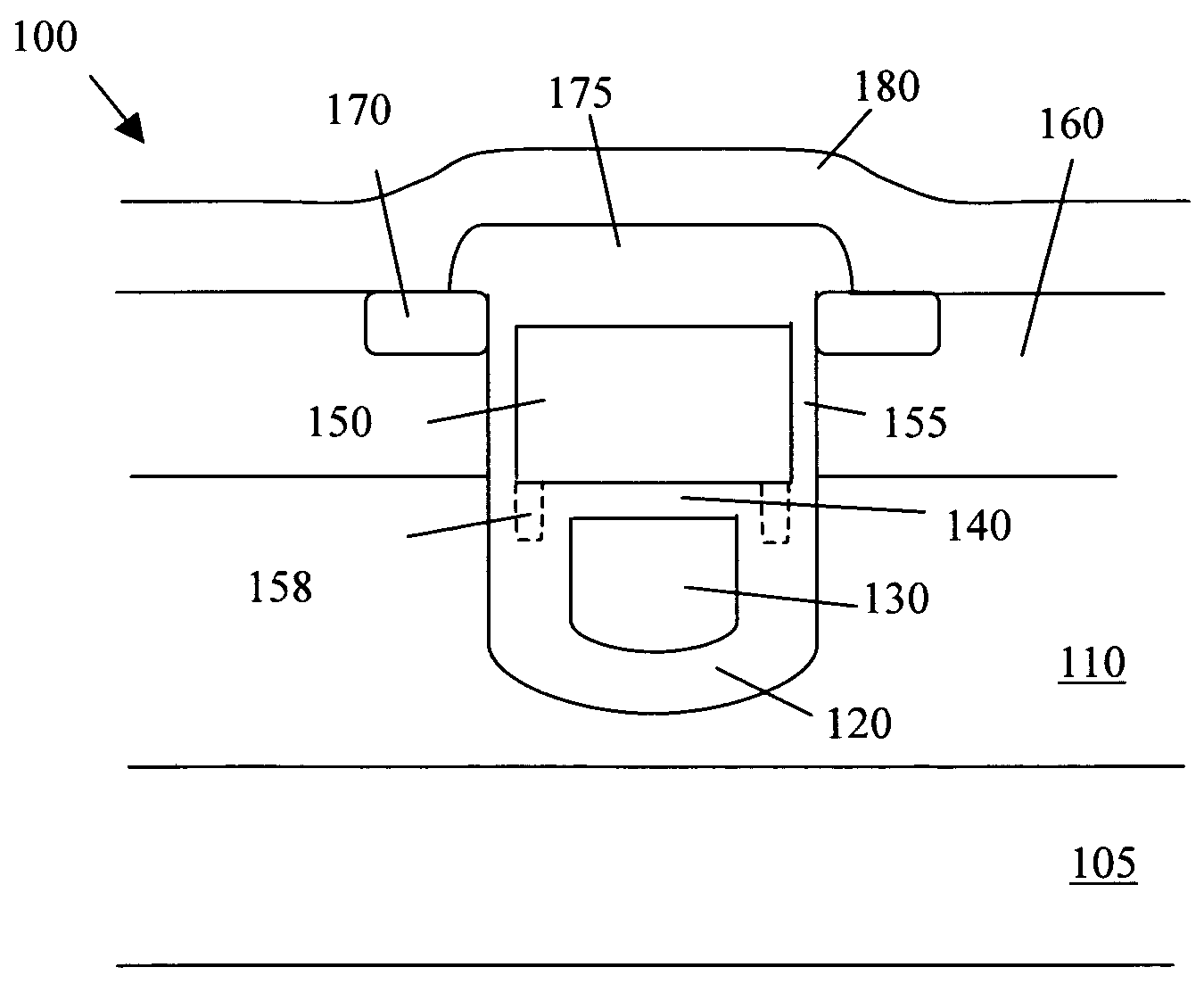
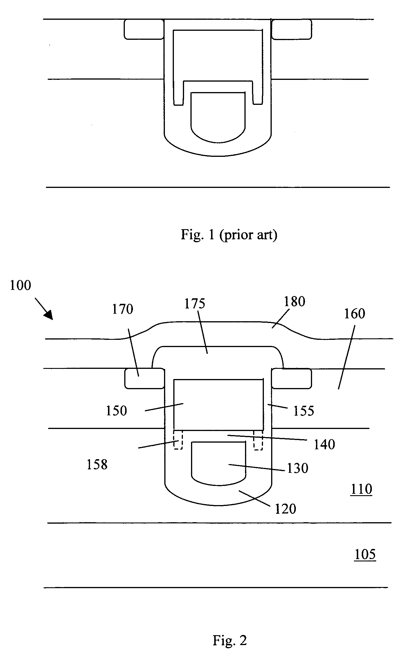
[0015]Referring to FIG. 2 for a cross sectional view of a trenched MOSFET device 100 of this invention. The trenched MOSFET device 100 is supported on a substrate 105 formed with an epitaxial layer 110. The trenched MOSFET device 100 includes a bottom gate segment 130 filled with polysilicon at the bottom portion below a top trenched gate segment 150. The bottom gate segment 130 filled with the polysilicon is shielded and insulated from a top gate segment 150 by an insulation inter-poly layer 140 disposed between the top and bottom segments. The bottom trenched-segment is also insulated from the drain disposed below 105 by the insulation layers 120 surrounding the bottom surface of the trenched gate. The top trenched gate segment 150 is also filled with a polysilicon layer in the top portion of the trench surrounded with a gate insulation layer 155 covering the trenched walls. The inter-poly insulation layer 140 is formed by HDP oxide deposition. The HDP deposition of the oxide laye...
PUM
 Abstract
Description
Claims
Application Information