Semiconductor device and manufacturing method of the same

a semiconductor and manufacturing method technology, applied in semiconductor devices, semiconductor/solid-state device details, electrical devices, etc., can solve the problems of reducing the yield rate, difficult to respond to the request for thinning of semiconductor devices, and not being able to stack semiconductor chips having the same chip siz

Inactive Publication Date: 2008-06-26
SOCIONEXT INC
View PDF13 Cites 62 Cited by
  • Summary
  • Abstract
  • Description
  • Claims
  • Application Information

AI Technical Summary

Benefits of technology

[0028]Accordingly, embodiments of the present invention may provide a novel and useful semiconductor device and manufacturing method of the same solving one or more of the problems discussed above.

Problems solved by technology

However, in the structure shown in FIG. 1, it is not possible to stack semiconductor chips having the same chip sizes.
Accordingly, in these structures, it is difficult to respond to the request for making the semiconductor device thin.
However, if the semiconductor chips are made thin, the yield rate may be reduced due to degradation of the strength of the semiconductor chip or reliability of the semiconductor device may be reduced.
Furthermore, manufacturing costs may be increased due to addition of manufacturing steps for making the semiconductor device thin.

Method used


Image

  • Semiconductor device and manufacturing method of the same
  • Semiconductor device and manufacturing method of the same
  • Semiconductor device and manufacturing method of the same

Examples


first embodiment

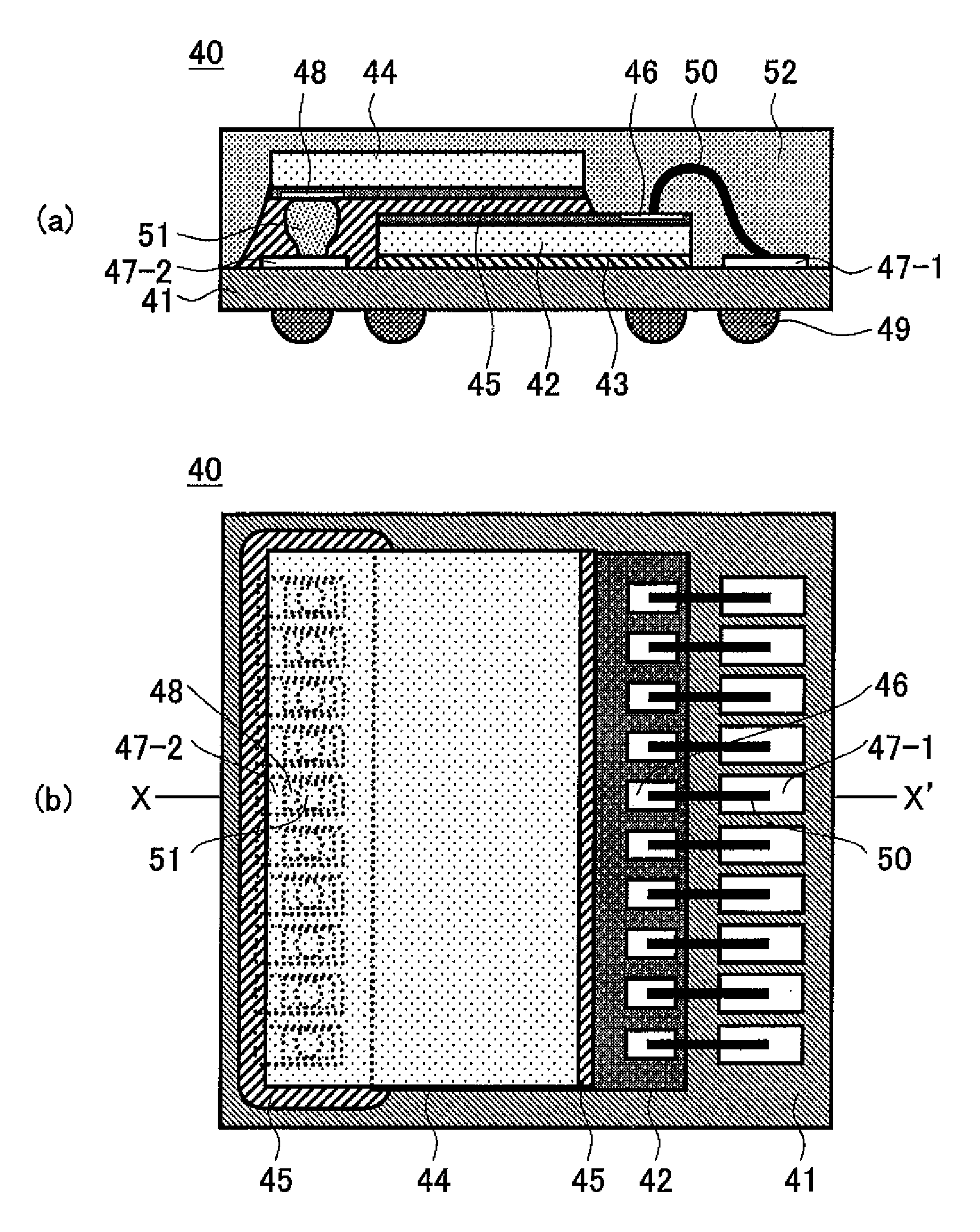
[0083]FIG. 5 shows a semiconductor device of a first embodiment of the present invention. FIG. 5(a) shows a cross section taken along line X-X′ of FIG. 5(b). In FIG. 5(b), illustration of a sealing resin is omitted.

[0084]A semiconductor device 40 of the first embodiment of the present invention has a structure of so-called a BGA (Ball Grid Array).

[0085]In other words, a first semiconductor chip (first semiconductor element) 42 is provided and fixed on a main surface of a wiring board 41 via a first adhesive 43. In addition, a second semiconductor chip (second semiconductor element) 44 is provided and fixed on the first semiconductor chip 42 via a second adhesive 45 in a so-called face down (flip chip) state.

[0086]On the above-mentioned main surface of the wiring board 41, plural first bonding pads 47-1 for connecting to the first semiconductor element are provided corresponding to electrode pads 46 of the first semiconductor chip 42, and plural second bonding pads 47-2 for connectin...

first modified example

[0116]A semiconductor device 60 of the first modified example of the first embodiment of the present invention is shown in FIG. 6.

[0117]In the semiconductor device 60, a minimum part such as the first bonding pad 47-1, the bonding wire 50, and the electrode pad 46 of the first semiconductor chip 42 is covered with sealing resin 62 made of, for example, thermosetting epoxy resin.

[0118]Thus, by covering the minimum part with the resin, this part can be protected from a mechanical external force, moisture, and the like and the amount of use of the sealing resin 62 can be reduced. Therefore, it is possible to reduce the manufacturing cost of the semiconductor device 60. As a method for selectively covering the sealing resin 62, a method whereby paste resin is supplied via a potting method can be used.

[0119]In the above-mentioned semiconductor device 60, the sealing resin 62 is not provided on a rear surface (upper surface in FIG. 6) of the second semiconductor chip 44 so that the rear s...

second modified example

[0120]A semiconductor device 70 of the second modified example of the first embodiment of the present invention is shown in FIG. 7.

[0121]In the semiconductor device 70, the first bonding pad 47-1, the bonding wire 50, the electrode pad 46 of the first semiconductor chip 42, a side surface of the first semiconductor chip 42, the second semiconductor chip 44, and the second adhesive 45 are covered with sealing resin 72. On the other hand, an upper surface of the second semiconductor chip 44 is not covered with the sealing resin 72 so as to be exposed outside.

[0122]Thus, since the first semiconductor chip 42 and the second semiconductor chip 44 are sealed in a body by the sealing resin 72 so as to be protected from a mechanical external force, moisture, and the like.

[0123]Furthermore, in this example as compared to the first modified example shown in FIG. 6, it is possible to form the external configuration with high precision and handle this easily.

[0124]In the above-mentioned semicon...


PUM


Abstract

A semiconductor device, includes a wiring board; a first semiconductor element mounted on the wiring board; a second semiconductor element mounted on the first semiconductor element so that a position of the second semiconductor element is shifted relative to a position of the first semiconductor element; wherein a part of a main surface of the second semiconductor element faces the first semiconductor element; and an electrode pad provided on the main surface of the second semiconductor element is connected to a second semiconductor element connection pad of the wiring board by a connection part.

Description

BACKGROUND OF THE INVENTION[0001]1. Field of the Invention[0002]The present invention generally relates to semiconductor devices and manufacturing methods of the same, and more specifically, to a semiconductor device wherein plural semiconductor elements are stacked on a wiring board and a manufacturing method of the semiconductor device.[0003]2. Description of the Related Art[0004]A chip stacked type semiconductor device which may be called a stacked package is known. In the chip stacked type semiconductor device, plural semiconductor chips (semiconductor elements) having different functions or plural semiconductor chips (semiconductor elements) having the same functions are stacked on a wiring board or a die pad of a lead frame. Each of electrode pads of the semiconductor chips and a bonding pad on the wiring board or an inner lead of the lead frame, are connected to each other by a bonding wire. Alternatively, the bonding wire connects the electrode pads to each other.[0005]In th...

Claims


Application Information

Patent Timeline
Patent Type & Authority Applications(United States)
IPC IPC(8): H01L23/48H01L21/58
CPCH01L2924/30105H01L2224/16145H01L24/13H01L24/29H01L2224/2919H01L2924/01006H01L2924/0665H01L2924/0132H01L2924/0133H01L2924/1579H01L2224/29111H01L2224/13111H01L25/0652H01L2224/73253H01L2224/92247H01L2224/48599H01L2924/10253H01L2924/12041H01L2224/26145H01L2224/26175H01L2224/0401H01L2224/45015H01L2224/45124H01L2224/45147H01L2924/13091H01L21/563H01L23/3128H01L24/16H01L24/27H01L24/32H01L24/45H01L24/48H01L24/49H01L24/73H01L24/743H01L24/83H01L24/91H01L25/0657H01L2224/05553H01L2224/1134H01L2224/1308H01L2224/13099H01L2224/16225H01L2224/27013H01L2224/32145H01L2224/32225H01L2224/45144H01L2224/48091H01L2224/48227H01L2224/49171H01L2224/49175H01L2224/73203H01L2224/73204H01L2224/73265H01L2224/743H01L2224/83051H01L2224/83191H01L2224/83192H01L2224/83194H01L2224/83856H01L2224/85201H01L2224/85205H01L2225/0651H01L2225/06517H01L2225/06555H01L2225/06562H01L2924/01004H01L2924/01005H01L2924/01013H01L2924/01014H01L2924/01028H01L2924/01029H01L2924/01033H01L2924/01042H01L2924/01047H01L2924/0105H01L2924/01074H01L2924/01077H01L2924/01078H01L2924/01079H01L2924/01082H01L2924/014H01L2924/07802H01L2924/09701H01L2924/14H01L2924/15311H01L2924/1815H01L2924/18161H01L2924/19042H01L2924/00014H01L2924/00H01L2924/3512H01L2924/00012H01L2924/0695H01L2924/20751H01L2924/20752H01L2924/20753H01L2924/181H01L2924/10161H01L2924/10162H01L2224/05624H01L2224/05647H01L2224/85444H01L2224/85447H01L2224/85455H01L2224/04042H01L2224/73215H01L24/05H01L2224/29015H01L2924/013H01L23/28
Inventor NISHIMURA, TAKAONARISAWA, YOSHIAKI
Owner SOCIONEXT INC
Why Eureka
Try Eureka