Semiconductor optical device, arrayed semiconductor optical device, and optical module

a semiconductor optical and array technology, applied in semiconductor lasers, instruments, optical elements, etc., can solve the problems of difficult control of the film thickness of the organic layer, deterioration of the yield in the manufacturing process, disconnection of the electrode, etc., and achieve the effect of reducing the parasitic capacitance and high design degree of freedom

Active Publication Date: 2017-05-04
LUMENTUM JAPAN INC
View PDF0 Cites 7 Cited by
  • Summary
  • Abstract
  • Description
  • Claims
  • Application Information

AI Technical Summary

Benefits of technology

[0022]According to the present invention, a semiconductor optical device, an arrayed semiconductor optical device, and an op

Problems solved by technology

However, in a case where an organic layer with a thick film such as the BCB is formed, it is not easy to control a film thickness of the organic layer.
In order to achieve sufficient decrease of capacitance, in general, a thickness of at least 1 μm to 3 μm is required for the organic layer and there is concern that deterioration of yield in the manuf

Method used


Image

  • Semiconductor optical device, arrayed semiconductor optical device, and optical module
  • Semiconductor optical device, arrayed semiconductor optical device, and optical module
  • Semiconductor optical device, arrayed semiconductor optical device, and optical module

Examples


first embodiment

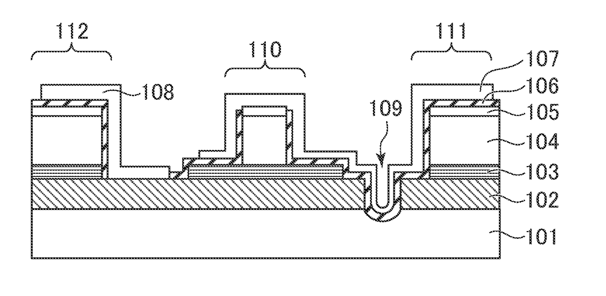
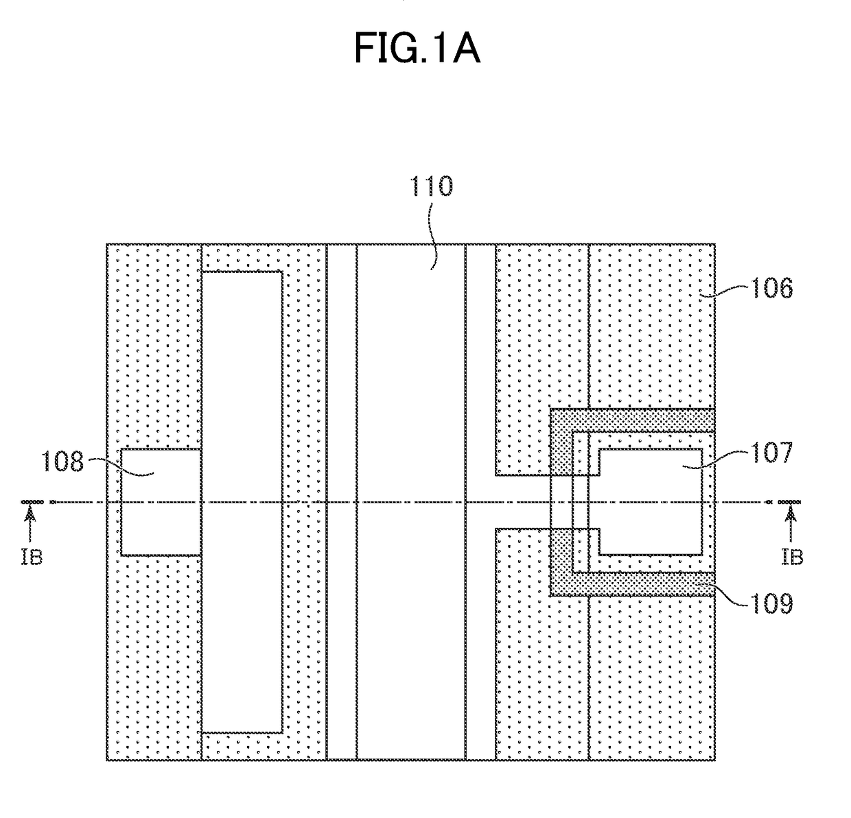
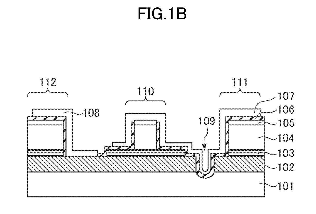
[0046]FIG. 1A is a plan view of a semiconductor optical device according to a first embodiment of the present invention. The semiconductor optical device according to the first embodiment is a ridge waveguide type distributed feedback (DFB) laser of a 1.3 μm wavelength band and includes a one-side electrode structure in which a p-side electrode 107 and an n-side electrode 108 are arranged on one side (here, upper surface) of a substrate. Aside surface existing on the upper end (upper side) of the semiconductor optical device of FIG. 1A corresponds to a front end surface and the semiconductor optical device emits light from the front end surface. The lower end (lower side) corresponds to a rear end surface.

[0047]FIG. 1B is a sectional view of the semiconductor optical device according to the first embodiment of the present invention and illustrates a section taken along the line IB-IB illustrated in FIG. 1A. As illustrated in FIG. 1B, the semiconductor optical device has a multilayer...

third embodiment

[0100]FIG. 4A is a plan view (diagram of an upper surface) of a semiconductor optical device according to a third embodiment of the present invention. FIG. 4B to FIG. 4D are sectional views of the semiconductor optical device according to the third embodiment of the present invention, and illustrate sections when taken along the lines IVB-IVB, IVC-IVC, and IVD-IVD illustrated in FIG. 3A, respectively. The semiconductor optical device according to the third embodiment has the same structure as that of the semiconductor optical device according to the second embodiment except that the structure of the laser part is a distributed reflector (DR) Laser (distribution reflector type laser) and a monitor photo detector (PD) is further included in the rear side of the laser part.

[0101]As illustrated in FIG. 4A, in the laser part of the semiconductor optical device according to the third embodiment, the light emitting part 110 which becomes a DFB laser area, a rear distributed Bragg reflector...

fourth embodiment

[0120]FIG. 5A is a plan view of an arrayed semiconductor optical device according to a fourth embodiment of the present invention. FIG. 5B is a sectional view of the arrayed semiconductor optical device according to the fourth embodiment of the present invention. The arrayed semiconductor optical device according to the embodiment is an arrayed semiconductor optical device in which a plurality of semiconductor optical devices according to the first embodiment are monolithically integrated at predetermined intervals and is an arrayed ridge waveguide type DFB laser. Here, the arrayed semiconductor optical device is a 4-channel DFB laser array. Each channel of the arrayed semiconductor optical device according to the fourth embodiment has the same structure as that of the semiconductor optical device according to the first embodiment. The ridges of the plurality of semiconductor optical devices of the arrayed semiconductor optical device according to the fourth embodiment are arranged ...


PUM


Abstract

Provided is a semiconductor optical device, an arrayed semiconductor optical device, an optical module having a structure to reduce the parasitic capacitance as well as a high design degree of freedom and having a multilayer structure in which a semi-insulating substrate, a first semiconductor layer having one conductive type, an active layer having light emission function, a second semiconductor layer having the other conductive type, an insulating layer, and a conductive layer are stacked in order from the bottom. The multilayer structure includes a light emitting structure, a first electrode structure, and a second electrode structure. In the semi-insulating substrate and the first semiconductor layer, a first grove which separates the second electrode structure from a remaining portion and approaches the second electrode structure with a non-linear shape rather than a linear shape in its entirety is formed.

Description

CROSS-REFERENCE TO RELATED APPLICATION[0001]The present application claims priority from Japanese application JP 2015-213207, filed on Oct. 29, 2015, the content of which is hereby incorporated by reference into this application.BACKGROUND OF THE INVENTION[0002]1. Field of the Invention[0003]The present invention is related to a semiconductor optical device, an arrayed semiconductor optical device, and an optical module, in particular, to reduction in parasitic capacitance of the semiconductor optical device.[0004]2. Description of the Related Art[0005]A semiconductor optical device having a one-side electrode structure in which one pair of electrodes is arranged on one surface of a substrate is used. A higher speed operation is required for the semiconductor optical device and thus, the parasitic capacitance of the semiconductor optical device needs to be reduced.SUMMARY OF THE INVENTION[0006]In “Design and Fabrication of Wide Wavelength Range 25.8-Gb / S, 1.3-μM, Push-Pull-Driven DM...

Claims


Application Information

Patent Timeline
IPC IPC(8): G02B6/42H01S5/125H01S5/343H01S5/40H01S5/22H01S5/12H01S5/185
CPCG02B6/4249H01S5/4025H01S5/22G02B6/4231H01S5/125G02B6/4286H01S5/343H01S5/0264H01S5/0267H01S5/1085H01S5/12H01S5/34306H01S5/42H01S5/0208H01S2301/176G02B6/4214H01S5/04257H01S5/02325H01S5/02251H01S5/185H01S5/0422
Inventor ADACHI, KOICHIRONAKAHARA, KOUJI
Owner LUMENTUM JAPAN INC
Why Eureka
Try Eureka