MEMS sensor, method of manufacturing MEMS sensor, and electronic apparatus

a manufacturing method and sensor technology, applied in the field of micro electro mechanical system sensor, can solve the problems that the inter-layer insulating layer between the two wiring layers the once formed inter-layer insulating layer cannot be used as a weight, etc., and achieves the effect of high accuracy and easy manufacturing

Active Publication Date: 2012-05-22
138 EAST LCD ADVANCEMENTS LTD
View PDF8 Cites 9 Cited by
  • Summary
  • Abstract
  • Description
  • Claims
  • Application Information

AI Technical Summary

Benefits of technology

[0008]An advantage of some aspects of the invention is to provide a MEMS sensor (for example, electrostatic capacitive acceleration sensor) in which the mass of a movable weight portion capable of moving in a direction perpendicular to a substrate can be efficiently increased, and a method of manufacturing the MEMS sensor, to provide a MEMS sensor that can detect a physical quantity such as acceleration with high accuracy, for example, and to provide a MEMS sensor that can be manufactured freely and easily by using a CMOS process in which multi-layer wiring is used, for example.
[0011]According to the aspect of the invention, the movable weight portion that is supported by coupling to the supporting portion via the connecting portion includes the movable electrode portion. Based on the fact that the facing distance between the movable-electrode face of the movable electrode portion and the facing-electrode face of the fixed electrode portion changes, the magnitude and direction of a physical quantity in the Z-direction perpendicular to the facing-electrode face can be detected from, for example, the relation between the magnitude and increase or decrease of a capacitance depending on the distance between the electrodes. In this case, the movable weight portion that can decrease sensitivity noise as the mass thereof increases can be formed as the stacked structure in which the plurality of conductive layers, the inter-layer insulating layer, and the plugs are closely stacked. Especially the plug having a large specific gravity in each of the layers is formed to have a columnar shape or a prismatic shape when the plug serves only for connection. However, since the plug is formed so as to include the wall portion formed in a wall shape along at least one axial direction on the two-dimensional surface parallel to the inter-layer insulating layer, the plug can contribute to an increase in the mass of the movable weight portion per unit area. Since the stacked structure constituting the movable weight portion can be formed by a typical CMOS process, the MEMS sensor can easily coexist with an integrated circuit portion on the same substrate. Moreover, since a multi-layer conductive layer is relatively easily formed, the degree of design freedom is high. For example, the demand for noise reduction of an acceleration sensor can be met by increasing the number of layers and increasing the mass of the movable weight portion.
[0012]The plugs are formed to be line-symmetric with respect to both the first direction and the second direction orthogonal to the first direction of the movable weight portion in a plan view, so that the movable balance of the movable weight portion is enhanced, and detection sensitivity can be further improved. The movable weight portion has the through hole for removing a lower layer by etching. By forming the plugs close to the through hole, the mass that is reduced by forming the through hole can be supplemented, and the detection sensitivity can be further improved.
[0014]As described above, since the stacked structure of the movable weight portion is suitable for a CMOS process, the MEMS sensor can be mounted together with the integrated circuit portion on the same substrate. This makes it possible to reduce a manufacturing cost compared to the case of manufacturing and assembling the respective ones in different processes. Further, the CMOS integrated circuit portion and the MEMS structure are formed monolithically, so that the wiring distance can be shortened. Therefore, it can be expected that a loss component due to the routing of the wiring will be reduced, and that resistance to external noise will be improved.
[0015]In the aspect of the invention, the fixed electrode portion can be formed of an impurity layer formed in the substrate. Accordingly, a first conductive layer (generally the same layer as a gate electrode) formed on the substrate is etched to form a second gap portion. Therefore, a second conductive layer and layers on the second conductive layer formed above the substrate can be used as the stacked structure, making it possible to increase the mass of the movable weight portion. Moreover, a polysilicon layer for forming the gate electrode of a transistor can be thin. When the polysilicon layer is etched to form the second gap portion, the gap between the electrodes forming a capacitance can be made small. Therefore, an electrode area for ensuring a predetermined capacitance can be made small, which contributes to the miniaturization of the MEMS sensor.
[0020]In the aspect of the invention, at least one of the movable-electrode face and the facing-electrode face, which is positioned on the second gap portion side, may be covered with an insulating layer formed by using a manufacturing process of the integrated circuit portion. This prevents the electrodes that form a capacitance from being in direct contact with each other to cause short. Moreover, by leaving an insulating layer in a lowermost layer of the movable electrode portion, the mass of the movable electrode portion can be increased.

Problems solved by technology

Since all inter-layer insulating layers are removed, the once formed inter-layer insulating layers cannot be used as a weight.
In addition, also an inter-layer insulating layer between the two wiring layers cannot be used as a weight.

Method used


Image

  • MEMS sensor, method of manufacturing MEMS sensor, and electronic apparatus
  • MEMS sensor, method of manufacturing MEMS sensor, and electronic apparatus
  • MEMS sensor, method of manufacturing MEMS sensor, and electronic apparatus

Examples


first embodiment

1. First Embodiment

[0051]In a first embodiment, the invention is applied to an acceleration sensor module for a Z-direction that is a vertical direction of a substrate, and a sensor chip and an IC chip are integrally formed by a wafer process.

1.1. MEMS Sensor

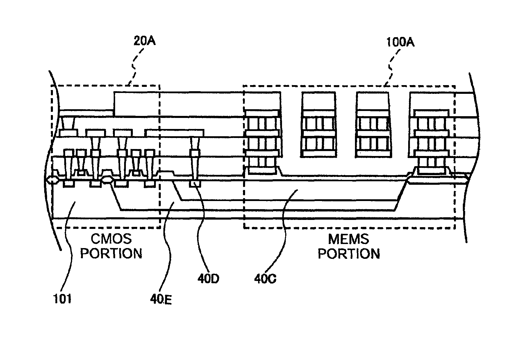
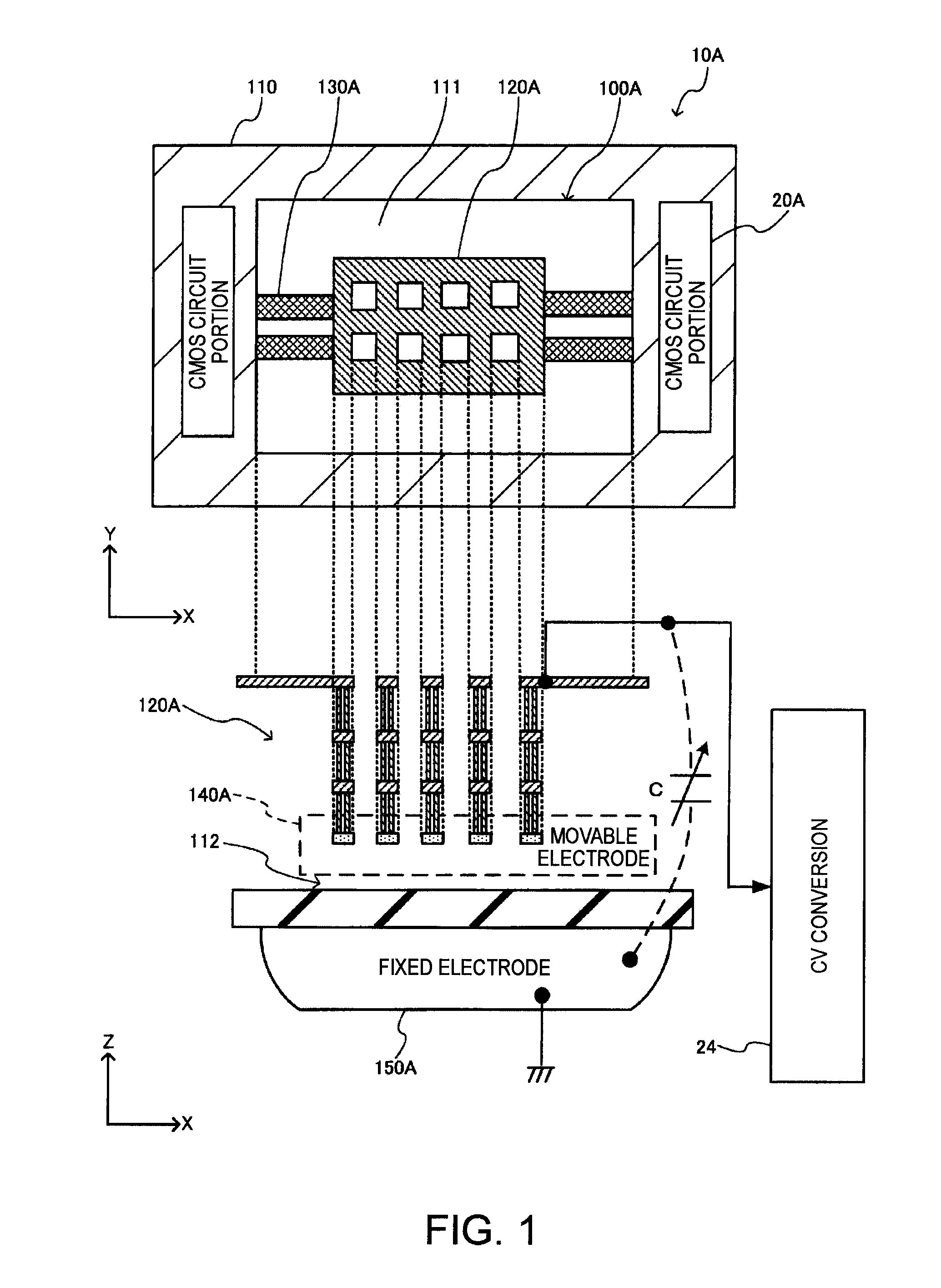
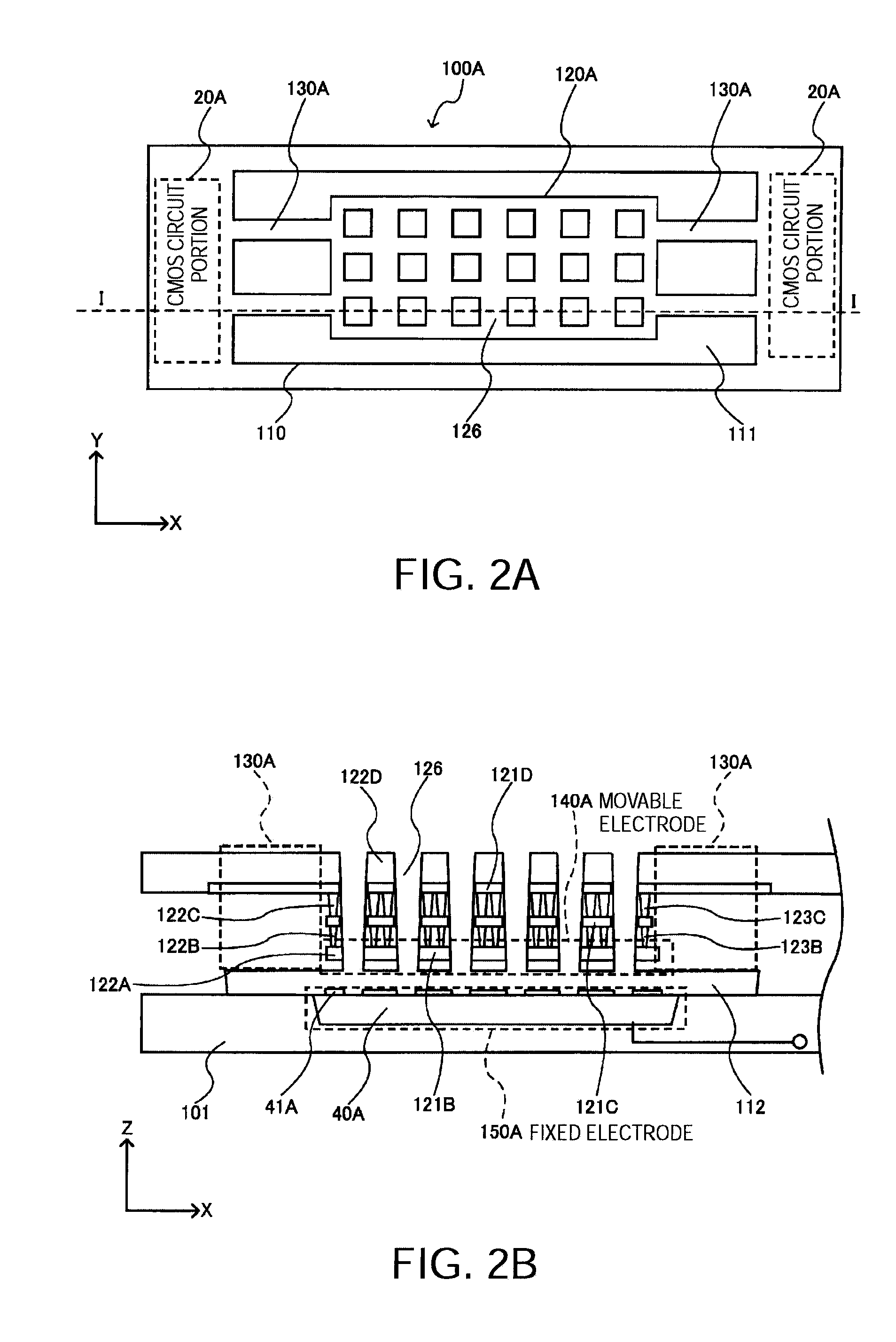
[0052]FIG. 1 is a schematic view of an acceleration sensor module 10A having mounted thereon a MEMS portion 100A according to the first embodiment to which a MEMS sensor of the invention is applied. The MEMS portion 100A according to the first embodiment has, for example, a movable weight portion 120A including a movable electrode portion 140A, a supporting portion 110 disposed around the movable weight portion 120A via first gap portions 111, a fixed electrode portion 150A having a facing-electrode face that faces a movable-electrode face of the movable electrode portion 140A via a second gap portion 112, and elastically deformable connecting portions 130A that support the movable weight portion 120A by coupling to the supporti...

second embodiment

2. Second Embodiment

[0101]With reference to FIGS. 18 to 22, a second embodiment of the invention will be described. In the following description, only the differences between the first embodiment and the second embodiment will be described. An acceleration sensor module 100B according to the second embodiment is a triaxial (X-, Y-, and Z-directions) acceleration sensor module to which the invention is applied. In the same manner as the first embodiment, a sensor chip and an IC chip can be integrally formed by a wafer process. In the second embodiment, the acceleration sensor 100B according to the embodiment has a movable weight portion 120B, different from the first embodiment where the MEMS portion 100A has the movable weight portion 120A.

[0102]The movable weight portion 120B is supported by a connecting portion 130B such that the movable weight portion can move in, in addition to the Z-direction orthogonal to the two-dimensional surface parallel to the substrate, at least one dire...


PUM

PropertyMeasurementUnit
thicknessaaaaaaaaaa
thicknessaaaaaaaaaa
thicknessaaaaaaaaaa

Abstract

A MEMS sensor includes: a substrate; a fixed electrode portion formed in the substrate; a movable weight portion formed above the fixed electrode portion via a gap; a movable electrode portion formed in the movable weight portion and disposed so as to face the fixed electrode portion; a supporting portion; and a connecting portion that couples the supporting portion with the movable weight portion and is elastically deformable, wherein the movable weight portion is a stacked structure having conductive layers and an insulating layer, and plugs having a larger specific gravity than the insulating layer are embedded in the insulating layer.

Description

BACKGROUND[0001]1. Technical Field[0002]The present invention relates to a MEMS (Micro Electro Mechanical System) sensor, a method of manufacturing the MEMS sensor, an electronic apparatus, and the like.[0003]2. Related Art[0004]As a silicon MEMS acceleration sensor with a CMOS integrated circuit for example, a reduction in size and cost for this type of MEMS sensor is rapidly progressing. The application and market of the MEMS sensor are expanding. In a main device form, an IC chip that converts a physical quantity into an electric signal and outputs the same is made into one package by a mounting process after a wafer process in most cases. For achieving an extreme reduction in size and cost, a technique of integrally forming a sensor chip and an IC chip by a wafer process is required (refer to JP-A-2006-263902).[0005]This type of MEMS sensor has such characteristics that sensitivity is enhanced as the mass of a movable weight portion increases. For increasing the mass of the mova...

Claims


Application Information

Patent Timeline
Patent Type & Authority Patents(United States)
IPC IPC(8): H01L29/84B81B3/00B81C1/00G01P15/125G01P15/18
CPCB81C1/00246G01P15/125G01P15/18G01P15/0802B81B2201/0235B81B2203/0109G01P2015/082
Inventor TAKAGI, SHIGEKAZUSATO, AKIRA
Owner 138 EAST LCD ADVANCEMENTS LTD
Why Eureka
Try Eureka