Defect inspection tool for sample surface and defect detection method therefor
- Summary
- Abstract
- Description
- Claims
- Application Information
AI Technical Summary
Benefits of technology
Problems solved by technology
Method used
Image

Examples
first embodiment
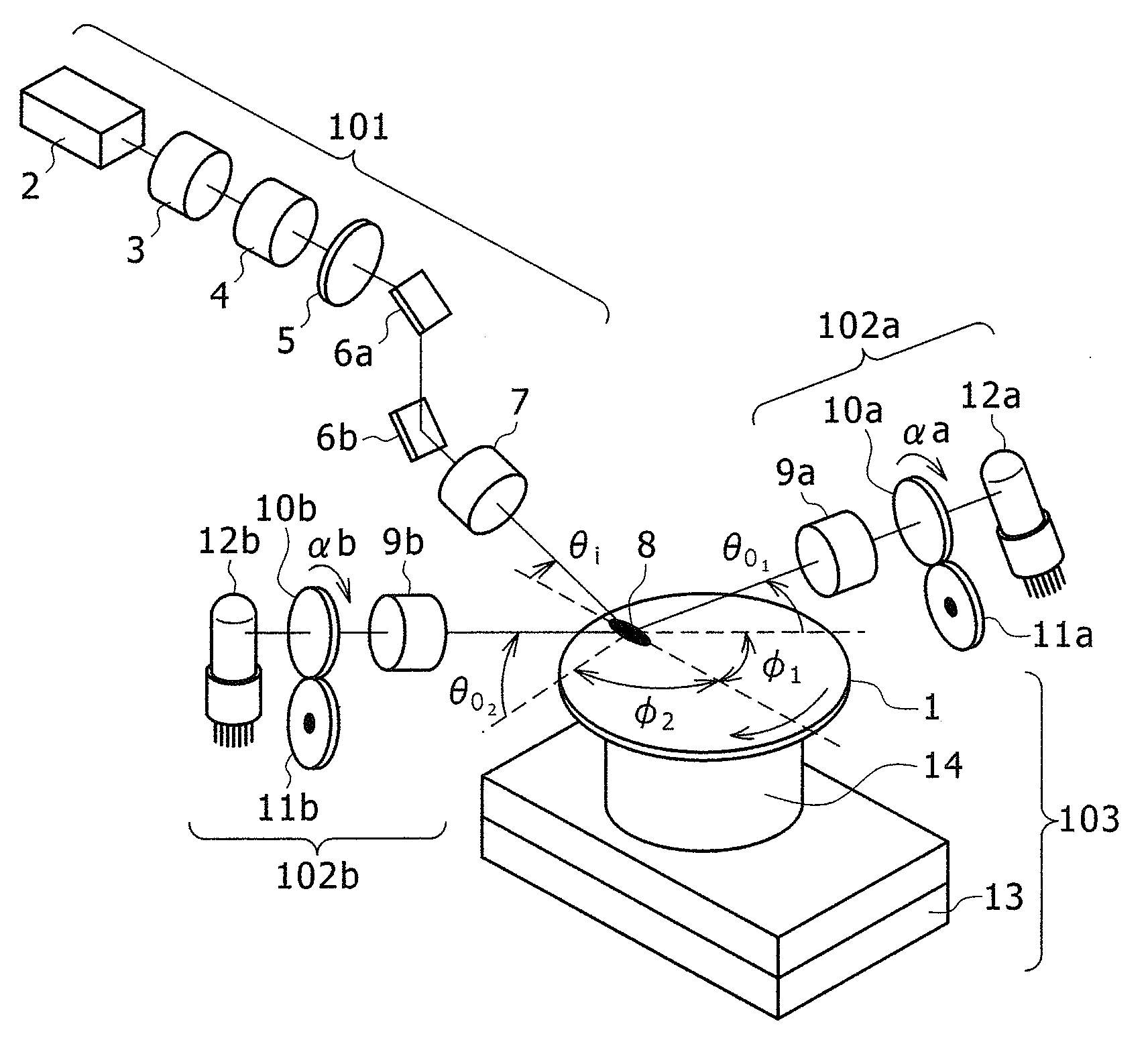
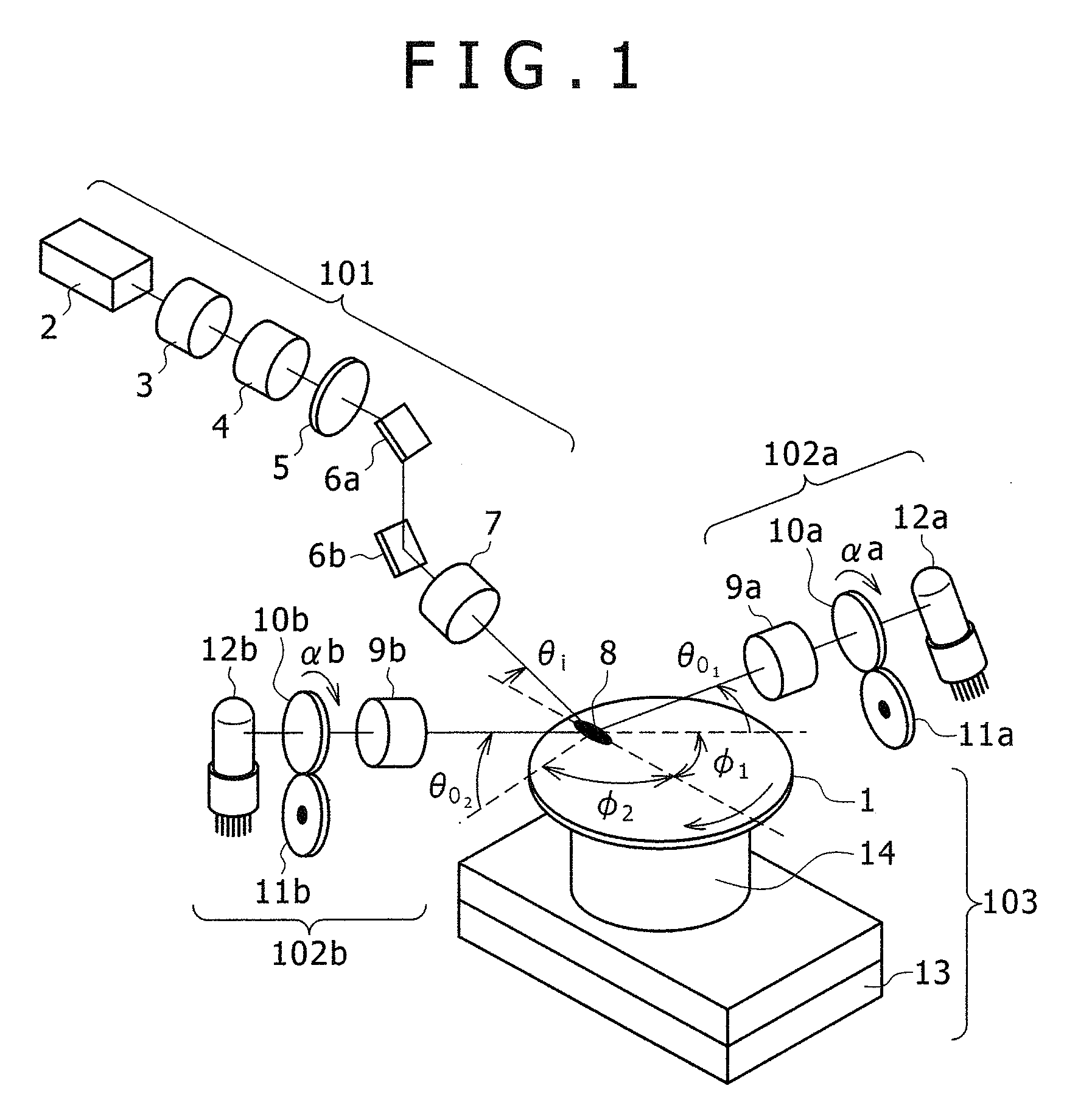
[0021]FIG. 2 shows one example of a tool for detecting a defect and a foreign substance on a semiconductor wafer according to the invention. FIG. 2 shows a case where a defect and a foreign substance on the semiconductor wafer before circuit pattern formation is detected. As schematic configuration, this tool is composed of an illumination optical system 101, detection optical systems 102, and a wafer stage 103. Two detection optical systems 102a and 102b are shown in FIG. 2. Note that the number of detection optical systems provided may be one or more.
[0022]The illumination optical system 101 is composed of a laser light source 2, an attenuator 3, a beam expander 4, a wavelength plate 5, and a condensing lens 7. A laser beam emitted from the laser light source 2 is adjusted to a required light amount by the attenuator 3, the beam diameter is expanded by the beam expander 4, and the polarization direction of illumination is set by the wavelength plate 5 to illuminate a detection are...
second embodiment
[0032]As described above, the optimum analyzer angle varies depending on the condition such as the detected angle of elevation (θ0), the detected angle of orientation (f), and the like. FIG. 1 shows one embodiment for this case. Tool configuration and an illumination optical system are the same as those of FIG. 2. One or more detection optical systems may be provided, as is the case with that of FIG. 1. An analyzer 10 to be inserted in the detection optical system is configured to be rotatable, and the rotation of the analyzer 10 is controlled by a rotating mechanism 11. This configuration permits constantly inspecting a foreign substance and a defect under optimum detection condition by controlling the angle (a) of the analyzer 10 even in a case where the detected angle of elevation (θ0), the detected angle of orientation (f), the complex refractive index of the film material, and the illumination condition (illumination angle of elevation θi and polarization direction) vary.
[0033]...
PUM
 Abstract
Description
Claims
Application Information
 - R&D Engineer
- R&D Manager
- IP Professional
- Industry Leading Data Capabilities
- Powerful AI technology
- Patent DNA Extraction
Browse by: Latest US Patents, China's latest patents, Technical Efficacy Thesaurus, Application Domain, Technology Topic.
© 2024 PatSnap. All rights reserved.Legal|Privacy policy|Modern Slavery Act Transparency Statement|Sitemap