Optical Element, Method for Production Thereof and Display Device

a technology of optical elements and display devices, applied in the direction of optical elements, photomechanical treatment, instruments, etc., can solve the problems of insufficient light diffusivity in this light diffusion sheet, inability to keep fine shape, and inability to achieve both well, so as to achieve good light diffusion performance and good light transmittance , the effect of less subject to environmental influen

Inactive Publication Date: 2008-06-26
ZEON CORP
View PDF9 Cites 10 Cited by
  • Summary
  • Abstract
  • Description
  • Claims
  • Application Information

AI Technical Summary

Benefits of technology

[0012]The optical element of the present invention has the precisely formed fine hologram surface diffusion pattern, has both the good light diffusion performance and the good light transmittance, is less subject to the environmental influence, and can be simply formed and in a large size. Since the display device of the present invent...

Problems solved by technology

Thus the diffusive performance and the transmittance are in trade-off relationship, that is, the both are not well-achieved.
However, the light diffusiveness is insufficient in this light diffusion sheet.
Thus, when the photosensitive material itself is used as the hologram surface diffusion pattern for the optical element, there has been a problem that the fine shape is...

Method used


Image

  • Optical Element, Method for Production Thereof and Display Device
  • Optical Element, Method for Production Thereof and Display Device
  • Optical Element, Method for Production Thereof and Display Device

Examples


example 1

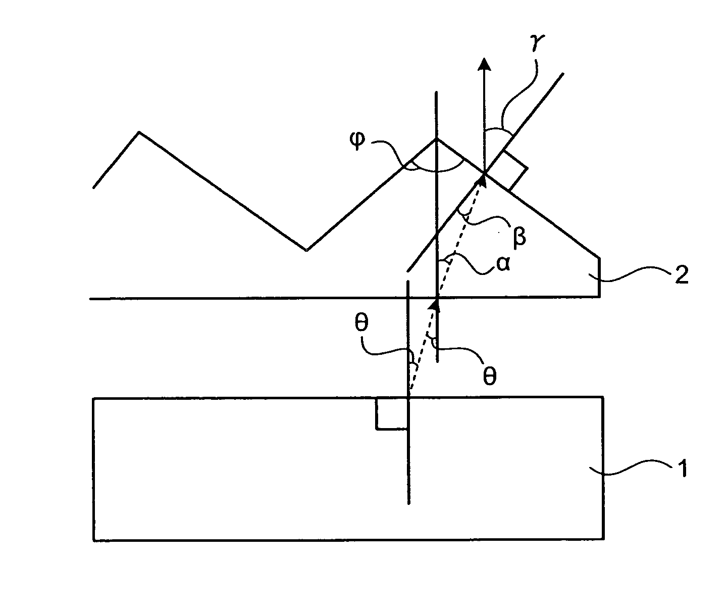
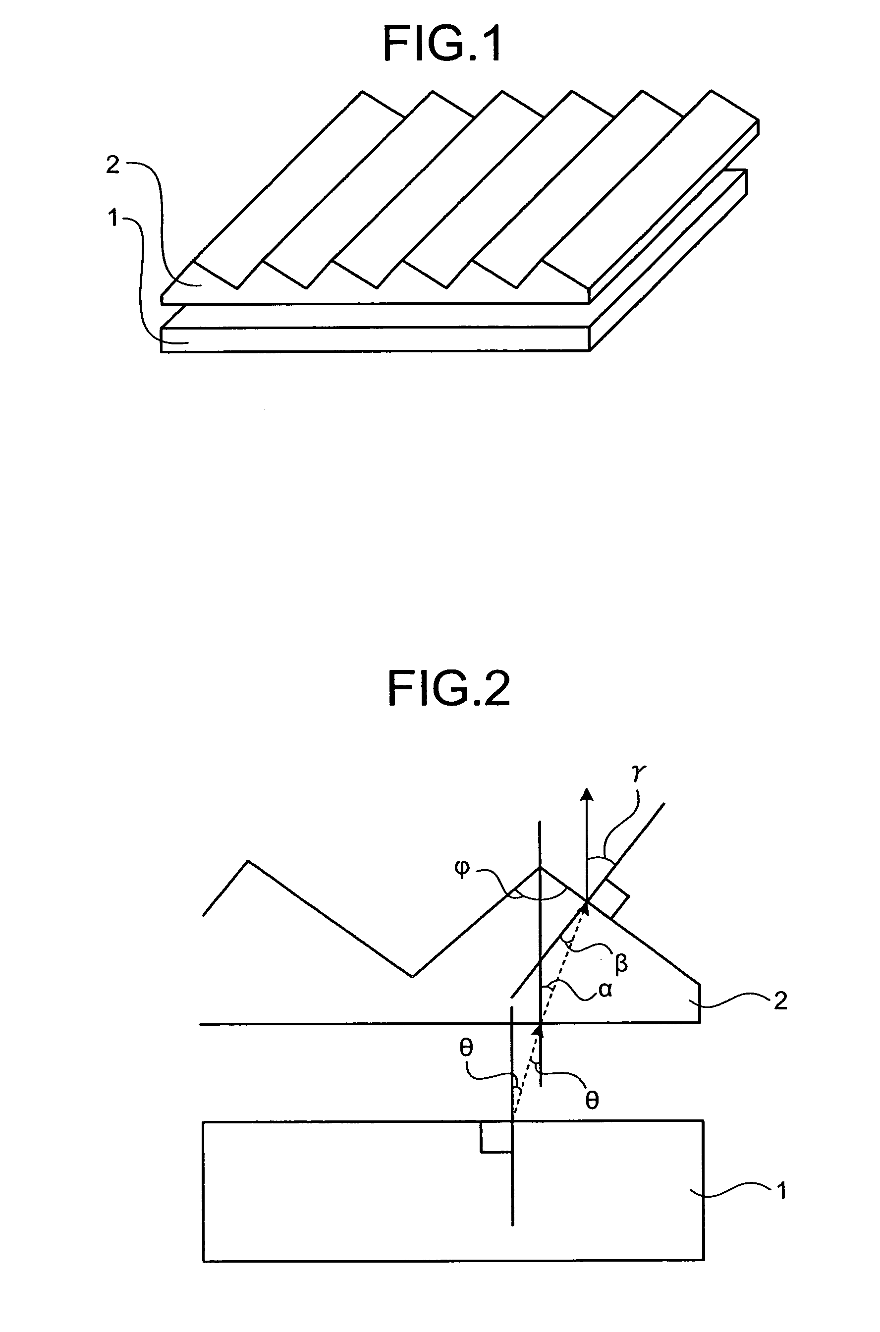
[0088]The stamper obtained in Preparative Example 2 was attached in a metal mold having a cavity of a length of 320.0 mm, a width of 426.0 mm and a depth of 2.0 mm, which was further attached to an injection-molding machine (mold clamping force: 3,430 kN). The DCP / ETD ring opening hydrogenated copolymer obtained in Preparative Example 1 was then injection-molded under the conditions of a cylinder temperature at 290° C., a mold temperature at 85° C., an injection speed at 100 mm / s and a cooling time for 50 seconds to form a 20 inch light diffusion plate (1) having the hologram surface diffusion pattern on one surface. The resulting light diffusion plate (1) was disposed on a surface table and an uplift height at a side face was measured using a micrometer caliper. Consequently the height was as small as 0.1 mm. Ra and Sm of the face having the hologram surface diffusion pattern on the resulting light diffusion plate (1) were measured, and consequently Ra, Sm and Ra / Sm were 2 μm, 4.8 ...

example 2

[0093]A liquid crystal television (2) was prepared in the same way as in Example 1 except that the light diffusion plate (1) in Example 1 was disposed so that the hologram surface diffusion pattern was on the surface facing the liquid crystal panel (opposed to the light source), and the luminance was measured. Consequently the average luminance and the luminance unevenness were 470 cd / m2 and 80%, respectively. When observed without the liquid crystal panel and the optical sheet, the images of the cold cathode tubes were scarcely observed on the light diffusion plate.

[0094]Further, the luminance was measured after leaving stand the above liquid crystal television (2) in the constant temperature and constant humidity bath at 60° C. and 90% RH (relative humidity) for 200 hours in the same way as in Example 1. Consequently, the average luminance and the luminance unevenness were 469 cd / m2 and 80%, respectively.

example 3

[0095]99.7 parts of the DCP / ETD ring-opening hydrogenated copolymer that has been produced in Preparative Example 1 and 0.3 parts of fine particles composed of crosslinked polysiloxane polymer (Tospearl 120, GE Toshiba Silicone) were mixed. The mixture was extruded using a biaxial extruder to be in a strand shape and cut using a pelletizer, to prepare pellets for the light diffusion plate. A light diffusion plate (2) was obtained by performing the injection-molding in the same way as in Example 1 except for using these pellets. Ra and Sm of the face having the hologram surface diffusion pattern on the resulting light diffusion plate (2) were measured, and consequently Ra, Sm and Ra / Sm were 2 μm, 4.8 μm and 0.41, respectively. The maximum value of the half value width of the light intensity of the resulting light diffusion plate (2) was 70°.

[0096]A liquid crystal television (3) was made in the same way as in Example 1 except that the light diffusion plate (2) was disposed so that the...


PUM


Abstract

The present invention is to provide an optical element in which both a good light diffusion performance and a good light transmittance are achieved and which is less subject to environmental influence, a method for production thereof and a display device using the optical element. An optical element including a molded body containing a resin having an alicyclic structure, wherein a fine hologram surface diffusion pattern has been precisely formed is provided. It is preferable that the optical element is a light diffusion plate or a light diffusion sheet. Further, it is preferable that the optical element is a molded body made by injection-molding.

Description

TECHNICAL FIELD[0001]The present invention relates to an optical element, a method for production thereof and a display device such as a flat-panel display device using the same. More particularly, the present invention relates to an optical element in which a fine hologram surface diffusion pattern has been precisely formed and which is less subject to environmental influence, a method for production thereof and a display device using the same.BACKGROUND ART[0002]Conventionally, as a means to control an output angle of light, optical elements to which various shapes are given on a surface of a transparent member are used in a display device using liquid crystal, EL and the like. It has been started to equip instruments such as mobile phones with an EL display device, and it is anticipated that the range of application of the EL display device will be expanded in the future. A liquid crystal display device has been widely used for many instruments such as mobile terminals, in-vehicl...

Claims


Application Information

Patent Timeline
IPC IPC(8): G03F1/06G03F1/92G02B5/02G02B5/04G02B5/32G02F1/1335
CPCG02B5/0252G02B5/0278G02F2001/133607G02B5/32G02B5/045G02F1/133607G02B5/02G02B5/20
Inventor HAYASHI, MASAHIKOSUZUKI, TOSHIAKITSUKADA, KEISUKESHIBUYA, AKIYOSHITAZAKI, SATOSHIOBUCHI, KAZUYUKI
Owner ZEON CORP
Why Eureka
Try Eureka