Sensor Device, Sensor System and Methods for Manufacturing Them

a sensor system and sensor technology, applied in the direction of interferometer acceleration measurement, instrumentation, and details of semiconductor/solid-state devices, can solve problems such as distortion or strain in the sensor body, and achieve the effects of reducing downsizing in the sensor system, facilitating downsizing, and facilitating the manufacture of sensor devices

Inactive Publication Date: 2008-07-03
MATSUSHITA ELECTRIC WORKS LTD
View PDF17 Cites 26 Cited by
  • Summary
  • Abstract
  • Description
  • Claims
  • Application Information

AI Technical Summary

Benefits of technology

[0024]In the sensor device and the sensor system of the present invention, the upper and lower sealing members housing the sensor body are made of the same material as that of the sensor body. Thus, there is no difference in thermal expansion coefficient between these components. This makes it possible to suppress temperature drift due to the difference in thermal expansion coefficient between the components of the sensor device. In one preferred embodiment of the sensor system, the sensor device and the integrated circuit are arranged in a stacked manner so that downsizing in the sensor system can be facilitated. In addition, the sensor-device manufacturing method of the present invention makes it possible to readily manufacture a sensor device having suppressed temperature drift. Further, the sensor-system manufacturing method of the present invention can reduce a thermal strain which is likely to remain in the sensor device after the manufacturing of the sensor system, to suppress deviation from design values of sensor characteristics.

Problems solved by technology

However; this technique involves a problem about distortion or strain in the sensor body 71 to be caused by temperature changes due to the large difference in thermal expansion coefficient between silicon and glass.

Method used


Image

  • Sensor Device, Sensor System and Methods for Manufacturing Them
  • Sensor Device, Sensor System and Methods for Manufacturing Them
  • Sensor Device, Sensor System and Methods for Manufacturing Them

Examples


first embodiment

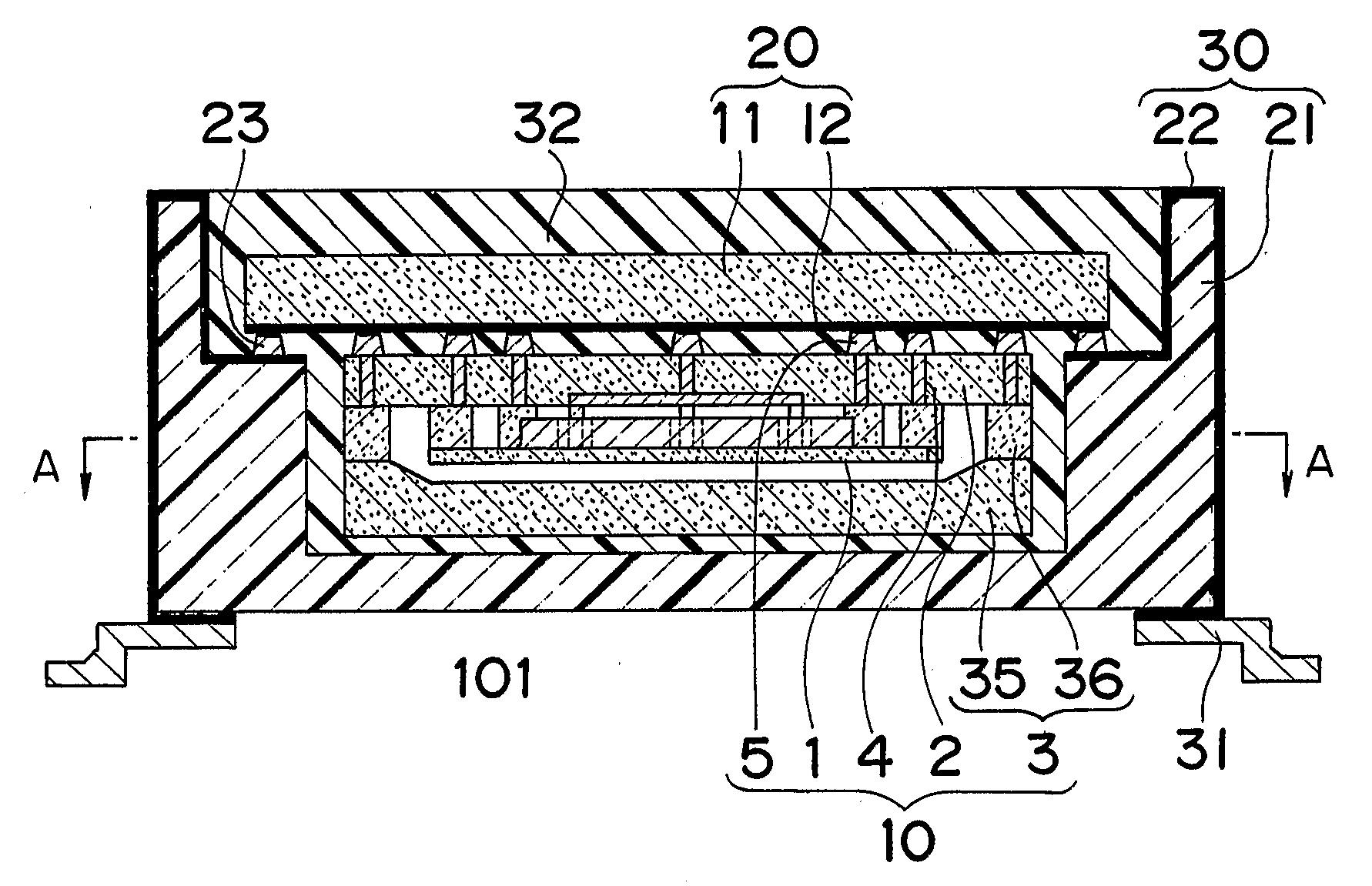
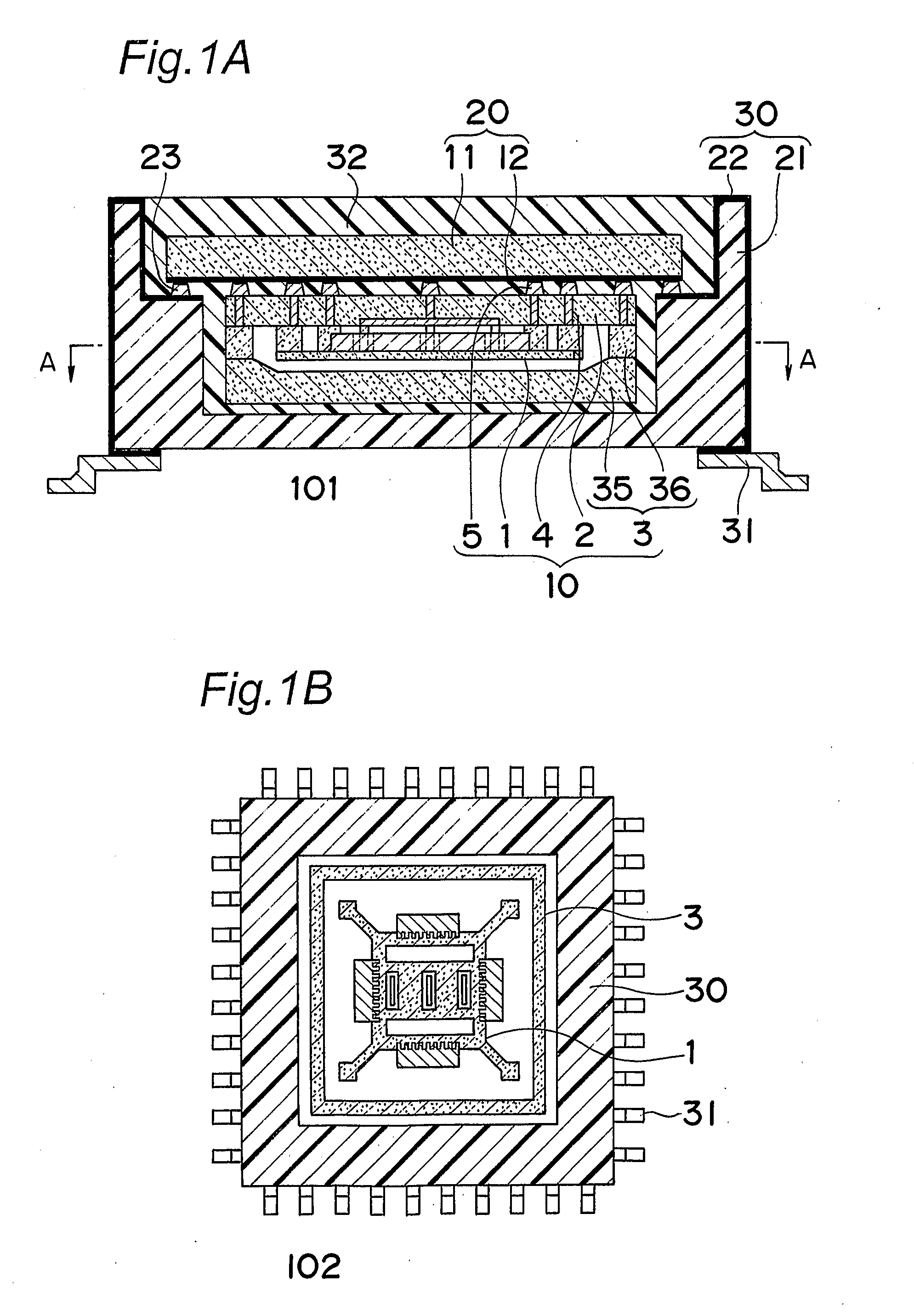
[0040]FIG. 1 is a sectional view showing the structure of a sensor system according to a first embodiment of the present invention, wherein FIG. 1A is a vertical sectional view of the sensor system, and FIG. 1B is a sectional view taken along the line A-A in FIG. 1A. This sensor system 101 is formed as an MEMS which includes a sensor device 10, an integrated circuit 20, an MID (Molded Interconnect Device) substrate 30, a mounting external electrode 31, and a sealing material 32. The sensor device 10 is designed to serve, for example, as an angular velocity sensor. The sensor device 10 includes a sensor body 1 made of a silicon-based material, an upper sealing member 2 made of a silicon-based material, and a lower sealing member 3 made of a silicon-based material. The term “silicon-based material” herein means that the material may include not only pure silicon but also impurity-doped silicon.

[0041]The upper sealing member 2 and the lower sealing member 3 are joined together to form ...

second embodiment

[0052]FIG. 3 is a vertical sectional view showing the structure of a sensor system according to a second embodiment of the present invention. In FIG. 3 and other figures, a component or element structurally or functionally identical to that in FIGS. 1A and 1B is defined by the same reference numeral or code, and its detailed description will be omitted. The sensor system 102 illustrated in FIG. 3 is mainly different from the sensor system 101 in FIGS. 1A and 1B, in that an MID substrate 30 is formed to interpose between a sensor device 10 and an integrated circuit 20 which are arranged in a stacked manner. The sensor device 10 is connected to a wiring pattern 22 through a mounting electrode 5, and the integrated circuit 20 is connected to the wiring pattern 22 through a mounting electrode 23. The MID substrate 30 is formed with an opening 25, and the wiring pattern 30 is also formed in the opening 25. Thus, the MID substrate 30 also relays the electrical connection between the senso...

third embodiment

[0055]FIG. 4 is a vertical sectional view showing the structure of a sensor system according to a third embodiment of the present invention. This sensor system 103 is mainly different from the sensor system 101 illustrated in FIGS. 1A and 1B, in that an anchor end of a mounting external electrode 31 is embedded in a substrate body 21 of an MID substrate 30. As with the sensor system 101, the mounting external electrode 31 in the sensor system 103 is formed as a stepwise bent pin. This structure can reduce a thermal strain which is likely to occur inside the sensor system 103 due to the difference in thermal expansion coefficient between the sensor system 103 and a circuit board onto which the sensor system 103 is mounted. Thus, the deterioration in sensor characteristics due to the thermal strain can be suppressed.

[0056]The mounting external electrode 31 may be embedded in the substrate body 21 by preparing a lead frame (not shown) having a number of mounting external electrodes 31 ...


PUM

PropertyMeasurementUnit
thicknessaaaaaaaaaa
thicknessaaaaaaaaaa
semiconductoraaaaaaaaaa

Abstract

A sensor system includes a sensor device (10) and an integrated circuit (20) for driving the device (10). The device (10) includes a sensor body (1) of a silicon-based material, an upper sealing member (2) of a silicon-based material and a lower sealing member (3) of a silicon-based material. The upper sealing member (2) and the lower sealing member (3) are joined together to cooperatively house the body (1) therewithin in an airtight manner. The device (10) and the circuit (20) are formed as a stacked body. The body (1) is electrically connected to a wiring pattern (12) of the circuit (20) through a conductive through-path (4) penetrating the upper sealing member (4) and a mounting electrode (5) provided on an outer surface of the upper sealing member (2). The device (10) is connected to an MID substrate (30) through the circuit (20).

Description

TECHNICAL FIELD[0001]The present invention relates to a sensor device, a sensor system and methods for manufacturing the sensor device and system.BACKGROUND ART[0002]A microsystem integrally including a microsize sensor or actuator fabricated using micromachining techniques based on semiconductor processes and a drive circuit (including a control circuit) therefor is known and described as “MEMS” (Micro Electro Mechanical System). FIG. 12 is a sectional side view of a conventional sensor system formed as a MEMS. This sensor system 150 includes a ceramic substrate 70, a sensor device 74, an integrated circuit 75, a mounting external electrode 77, and a sealing material 78. The ceramic substrate 70 has a wiring pattern 76.[0003]The sensor device 74 is designed to serve as an angular velocity sensor which includes a sensor body 71 made of a silicon-based material, an upper sealing member 72 made of glass, and a lower sealing member 73 made of glass. The upper and lower sealing members ...

Claims


Application Information

Patent Timeline
Patent Type & Authority Applications(United States)
IPC IPC(8): G01C19/00G01P1/02G01P9/04G01P15/08H01L23/02H01L23/06H01L29/84
CPCB81B7/0048B81B7/007B81B2207/012B81B2207/096Y10T29/49002B81C1/0023G01P1/023G01P15/0802B81B2207/097H01L2224/16225H01L23/06H01L23/02
Inventor TSUJI, KOJISANAGAWA, YOSHIHARUKIRIHARA, MASAOGOUDA, KAZUONISHIJIMA, YOUICHI
Owner MATSUSHITA ELECTRIC WORKS LTD
Why Eureka
Try Eureka