Etching apparatus using neutral beam and method thereof

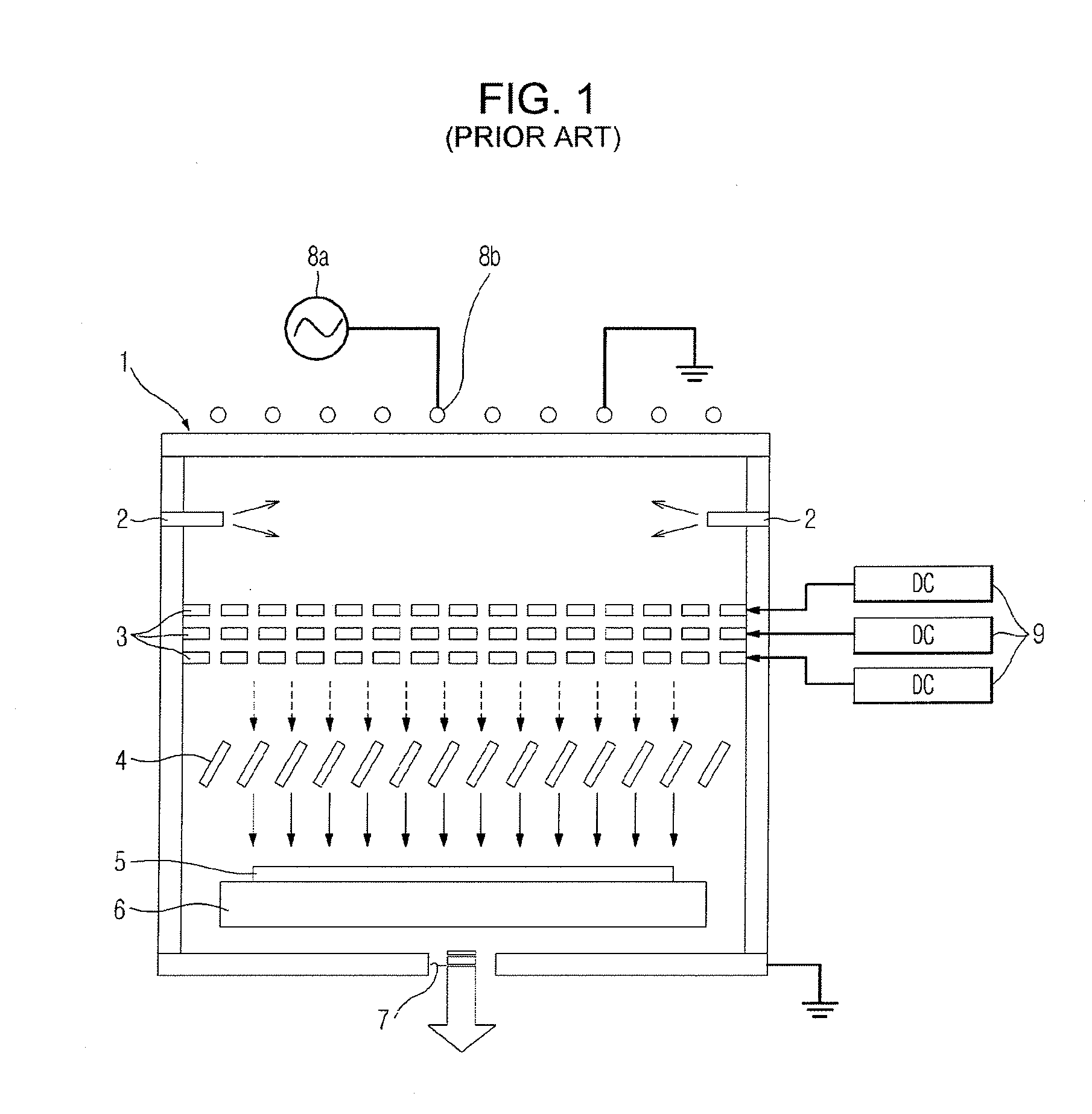
a technology of neutral beam and etching apparatus, which is applied in the direction of electrical apparatus, electrical discharge tubes, decorative arts, etc., can solve the problems of reducing the life span of reflection plates b>4/b>, generating foreign substances, physical and electrical damage to semiconductor wafers or specific material layers, etc., and achieves high neutralizing efficiency and not causing directionality and energy loss.

Inactive Publication Date: 2008-07-03
SAMSUNG ELECTRONICS CO LTD
View PDF1 Cites 188 Cited by
  • Summary
  • Abstract
  • Description
  • Claims
  • Application Information

AI Technical Summary

Benefits of technology

[0011]The general inventive concept provides an etching apparatus using a neutral beam, in which an ion beam extracted from plasma is converted into a neutral beam without physically colliding with a neutralization unit to prevent damage to the neutralization unit and generation of foreign substances due to a collision, thus having a high neutralizing efficiency and not causing directionality and energy losses.

Problems solved by technology

The ions collide with a semiconductor wafer, or a specific material layer on the semiconductor wafer, with energy of several hundreds of eV, thus causing physical and electrical damage to the semiconductor wafer or the specific material layer.
However, the above conventional etching apparatus has several problems, such as the reduced life span of the reflection plates 4 due to the physical collision with the ion beam extracted from the plasma, the generation of foreign substances due to the collision, and the generation of energy and directionality losses due to neutralization.

Method used


Image

  • Etching apparatus using neutral beam and method thereof
  • Etching apparatus using neutral beam and method thereof
  • Etching apparatus using neutral beam and method thereof

Examples


Embodiment Construction

[0034]Reference will now be made in detail to the embodiments of the present general inventive concept, an example of which is illustrated in the accompanying drawings, wherein like reference numerals refer to like elements throughout. The embodiments are described below to explain the present general inventive concept by referring to the annexed drawings.

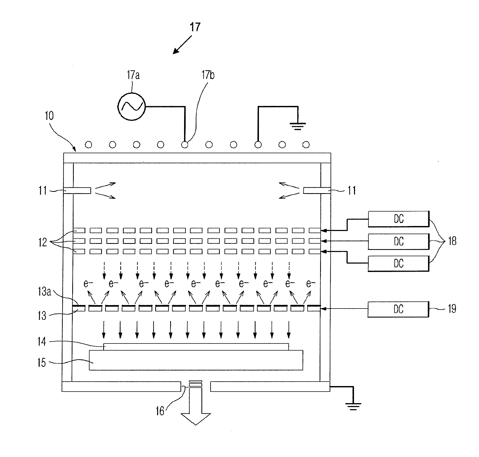
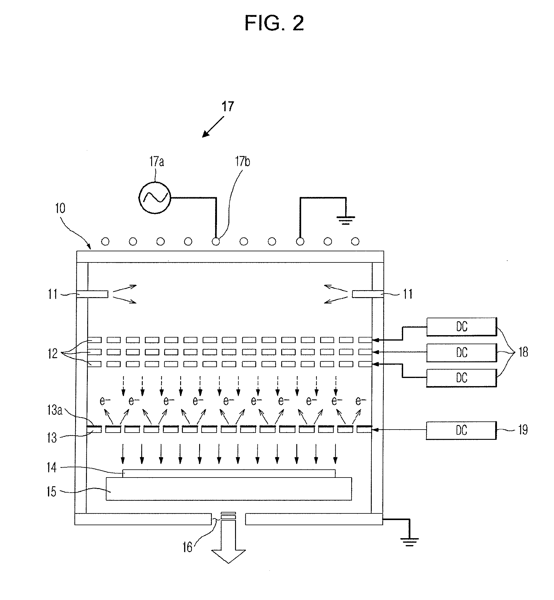
[0035]As illustrated in FIG. 2, an etching apparatus using a neutral beam in accordance with an embodiment of the present general inventive concept includes a chamber unit 10 divided into a source chamber and a process chamber, gas supply units 11, an ion extraction unit having a plurality of grids 12 and a first DC power source unit 18, an electron emission unit having electron emission electrode 13, an electron emission layer 13a and a second DC power source unit 19, a chuck 15, and a gas exhaust port 16, and a high-frequency power source unit 17.

[0036]The chamber unit 10 is divided into the source chamber which is located at an ...


PUM

PropertyMeasurementUnit
DC poweraaaaaaaaaa
electric potentialaaaaaaaaaa
diameteraaaaaaaaaa

Abstract

An etching apparatus using a neutral beam includes an electron emission unit to convert an ion beam, extracted from plasma by a plurality of grids, into a neutral beam by colliding the ion beam with electrons to prevent the ion beam from physically colliding with the electron emission unit, thus preventing the damage to a neutralization unit and generation of foreign substances with a simple structure. Further, the etching apparatus converts the ion beam into the neutral beam at a high neutralizing efficiency without causing directionality and energy losses, and generates a neutral beam having a large area, thus uniformly etching a semiconductor wafer.

Description

CROSS-REFERENCE TO RELATED APPLICATIONS[0001]This application priority under 35 U.S.C. § 119(a) from Korean Patent Application No. 2007-0000674, filed Jan. 3, 2007, in the Korean Intellectual Property Office, the disclosure of which is incorporated herein in its entirety by reference.BACKGROUND OF THE INVENTION[0002]1. Field of the Invention[0003]The present general inventive concept relates to an etching apparatus using a neutral beam, and more particularly, to an etching apparatus using a neutral beam, which etches a target object, such as a semiconductor wafer, by converting an ion beam extracted from plasma into a neutral beam, and a method thereof.[0004]2. Description of the Related Art[0005]As integration of semiconductor devices has increased in demand, design of smaller semiconductor integrated circuits has resulted in the production of semiconductor integrated circuits with a critical dimension of less than 0.25 μm. In order to design the above microscopic semiconductor dev...

Claims


Application Information

Patent Timeline
Patent Type & Authority Applications(United States)
IPC IPC(8): C23F1/00B44C1/22
CPCH01J37/32357H01J37/3233H01L21/3065
Inventor JEON, YUN KWANGLEE, JIN SEOKLEE, YUNG HEEKIM, GI TAE
Owner SAMSUNG ELECTRONICS CO LTD
Why Eureka
Try Eureka