Single-Chip Monolithic Dual-Band Visible- or Solar-Blind Photodetector

a monolithic, visible or solar-blind technology, applied in the direction of optical radiation measurement, radiation control devices, instruments, etc., can solve the problems of high sensitivity of photomultiplier tubes (pmts), low mechanical and temperature strength, and high voltage operation

Inactive Publication Date: 2008-07-03
INTEGRATED MICRO SENSORS
View PDF3 Cites 56 Cited by
  • Summary
  • Abstract
  • Description
  • Claims
  • Application Information

AI Technical Summary

Problems solved by technology

Currently used photomultiplier tubes (PMTs) have high sensitivity, but are bulky, require high voltage operation, and have low mechanical and temperature strength.
Some recently developed flame detectors are composed of discrete UV and IR solid-state components in one housing, but these devices sustain temperatures only up to 125° C., and are not capable of detecting multi-band optical signals with high spatial resolution.
Several attempts to develop UV detector structures on diamond were made by 1996, but lack of high quality layers and insufficient doping levels did not result in practical devices.
Visible-blind UV photodetectors have been fabricated on silicon carbide (SiC) substrates, but the technology is relatively immature due to the absence of high quality large area substrates until recent years.
In the area of IR detection, the conventional HgCdTe- and InSb-based detectors display high quantum efficiencies but are difficult to integrate into large arrays.

Method used


Image

  • Single-Chip Monolithic Dual-Band Visible- or Solar-Blind Photodetector
  • Single-Chip Monolithic Dual-Band Visible- or Solar-Blind Photodetector
  • Single-Chip Monolithic Dual-Band Visible- or Solar-Blind Photodetector

Examples


Embodiment Construction

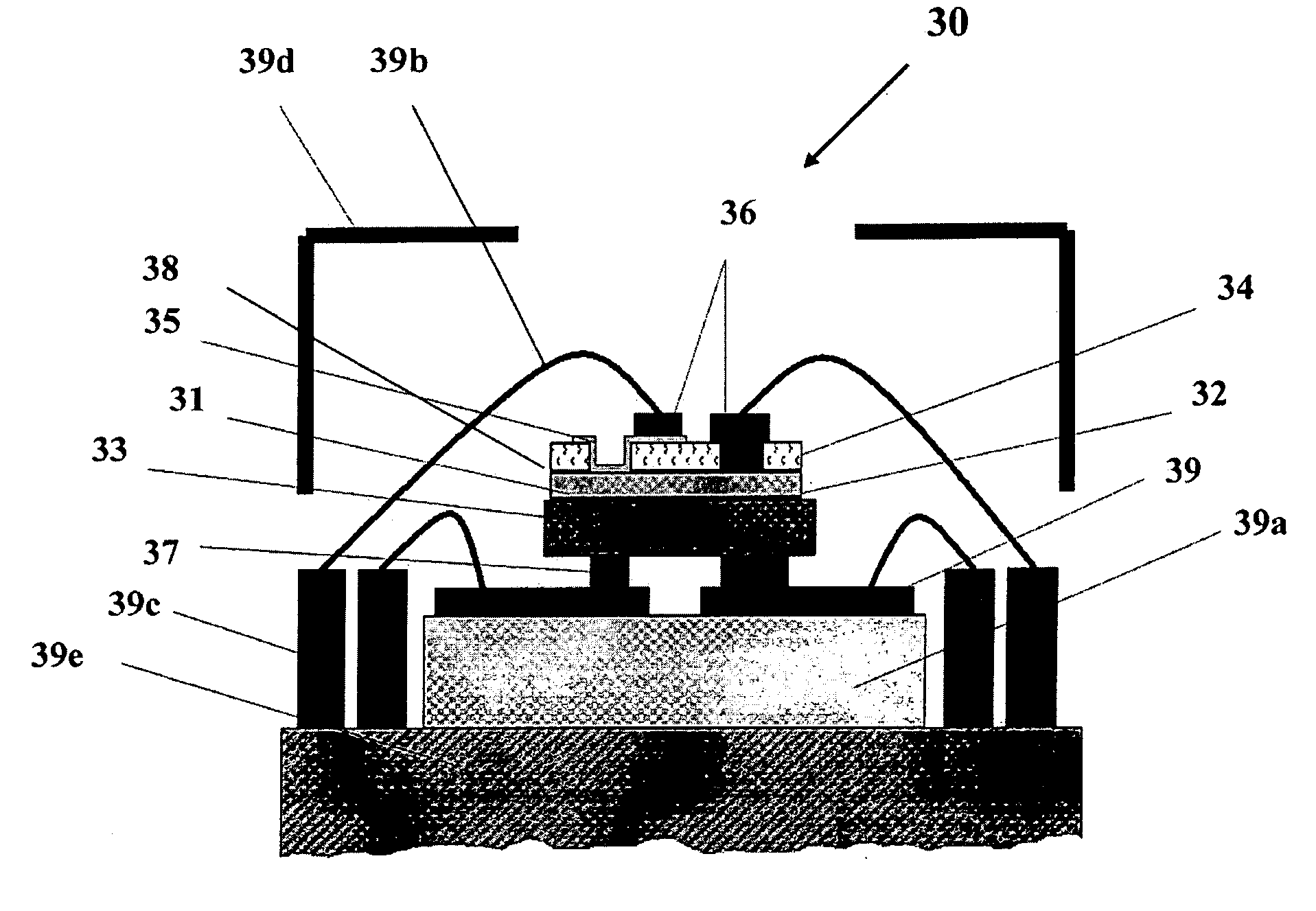
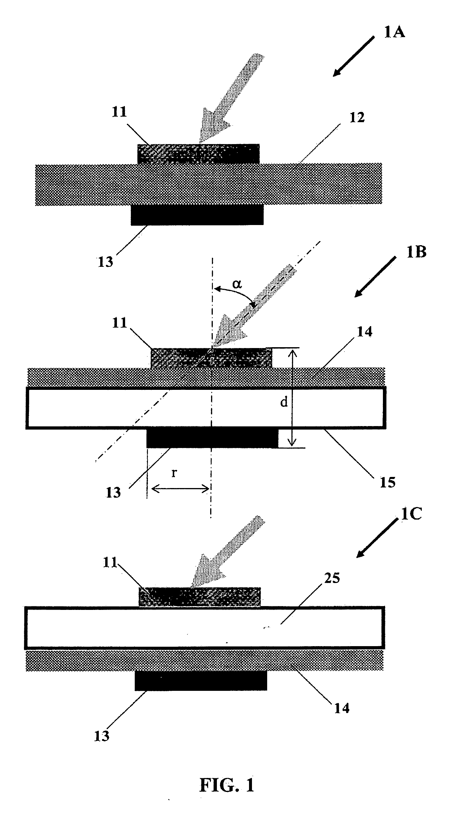
[0028]The device disclosed herein meets the following basic requirements:[0029]1) two photosensitive structures are stacked on a single substrate to form a monolithic photodetector;[0030]2) one structure is sensitive to radiation in a UV band and the second structure is sensitive to radiation in an IR band;[0031]3) The UV sensitive area on the front side of the photodetector is vertically aligned with the IR sensitive area on the back side of the photodetector, as shown in FIG. 3.[0032]3) the monolithic photodetector is insensitive to solar or visible radiation;[0033]4) the monolithic photodetector is capable of time- and electrically-resolved detection of both UV and IR radiation in the same space register;[0034]5) the two active semiconductor layers and contacts used as photosensitive structures as well as the passive semiconductor layer to filter out the visible or solar radiation, are stacked on a single substrate in one embodiment;[0035]6) the photosensitive structures are eith...


PUM


Abstract

A photodetector having sensitivity in a wide temperature range in both an infrared and an ultraviolet band is provided. The photodetector is formed on a single chip and is designed to be blind to solar or visible radiation. Structures disclosed allow fast and efficient detection of signals with high spatial and temporal resolution. Such sensors may be used for multi-pixel focal arrays and applied for fire detection applications, various space- and military-related applications and other applications. A method for increasing rejection of visible light by the IR sensitive material is also provided.

Description

[0001]This is a continuation-in-part application of application Ser. No. 11 / 403,691, filed Apr. 13, 2006BACKGROUND OF THE INVENTION[0002]1. Field of the Invention[0003]The present invention relates to monolithic visible- or solar-blind photodetectors with resolved sensitivities in the UV and IR bands. Methods for fabrication of the photodetectors and a method for decreasing sensitivity of the integrated structure to visible or solar radiation are also provided.[0004]2. Description of Related Art[0005]Solid-state optical detectors based on semiconductor materials have replaced photoemissive devices in a wide variety of both commercial and military applications due to their broad spectral responsivity, excellent linearity, high quantum efficiency, high dynamic range of operation, and possibility of large-format image arrays. The spectral range of most semiconductor-based optical detectors is determined by optical absorption in the active semiconductor material layer at energies above ...

Claims


Application Information

Patent Timeline
Patent Type & Authority Applications(United States)
IPC IPC(8): H01L31/00
CPCH01L31/09H01L31/1035H01L31/101
Inventor STARIKOV, DAVIDBENSAOULA, ABDELHAK
Owner INTEGRATED MICRO SENSORS
Why Eureka
Try Eureka