Integrated tunable micro-antenna with small electrical dimensions and manufacturing method thereof

a micro-antenna and electrical dimension technology, applied in the direction of waveguide devices, electrical apparatus, structural forms of radiation elements, etc., can solve the problems of reducing efficiency and bandwidth, reducing the physical dimension of such planar structures, and reducing so as to achieve significant antenna size reduction and increase the capacity of being tunable

Inactive Publication Date: 2008-07-03
UNIVERSITY OF MINHO
View PDF7 Cites 24 Cited by
  • Summary
  • Abstract
  • Description
  • Claims
  • Application Information

AI Technical Summary

Benefits of technology

[0018]The main goal of the present invention is to provide a multilayer micro-antenna, electrically small, capable of being co-integrated with the...

Problems solved by technology

However, for some applications, like the IEEE 802.11 standards or Bluetooth, the physical dimension of such planar structures may be too big, turning impossible its integration inside the radio-frequency (RF) devices.
However, this technique leads usually to low efficiency and bandwidth reduction.
Due to limitations of available room, imposed by the dimensions of the integrated circuits and due to the necessity to reduce the device dimensions, there has been for a long time the necessity of developing an antenna with an adequate geometry and dimension for integration inside RF integrated circuits (IC).
Until now, the integration of antennas has been mainly based on the usage of the conventional microstrip antenna, being its integration limited to applications at higher frequencies.
This happens because most of the proposed solutions to reduce the antenna size do not always impose as restriction the utilization of geometry, materials and manufacturing methods compatible with the integration of such an antenna in an integrated RF IC device.
In this way, the project of compact and fully integrated antennas is still a challenge the industry wishes to solve to allow the development of modern RF devices with wireless communications.
Due to the physical limitations associated to RF devices, an integrated antenna must have an electrical small dimension, and must work on a limited ground plane, which has a significant influence on the return losses and may also provoke a reduction of the antennas' front/back ratio.
However, due to the antennas' geometry and structure, its integration, using conventional packaging techniques, is not possible.
Furthermore, the use of the simple multilayer technique does not provide an antenna with small enough dimensions for...

Method used


Image

  • Integrated tunable micro-antenna with small electrical dimensions and manufacturing method thereof
  • Integrated tunable micro-antenna with small electrical dimensions and manufacturing method thereof
  • Integrated tunable micro-antenna with small electrical dimensions and manufacturing method thereof

Examples


Embodiment Construction

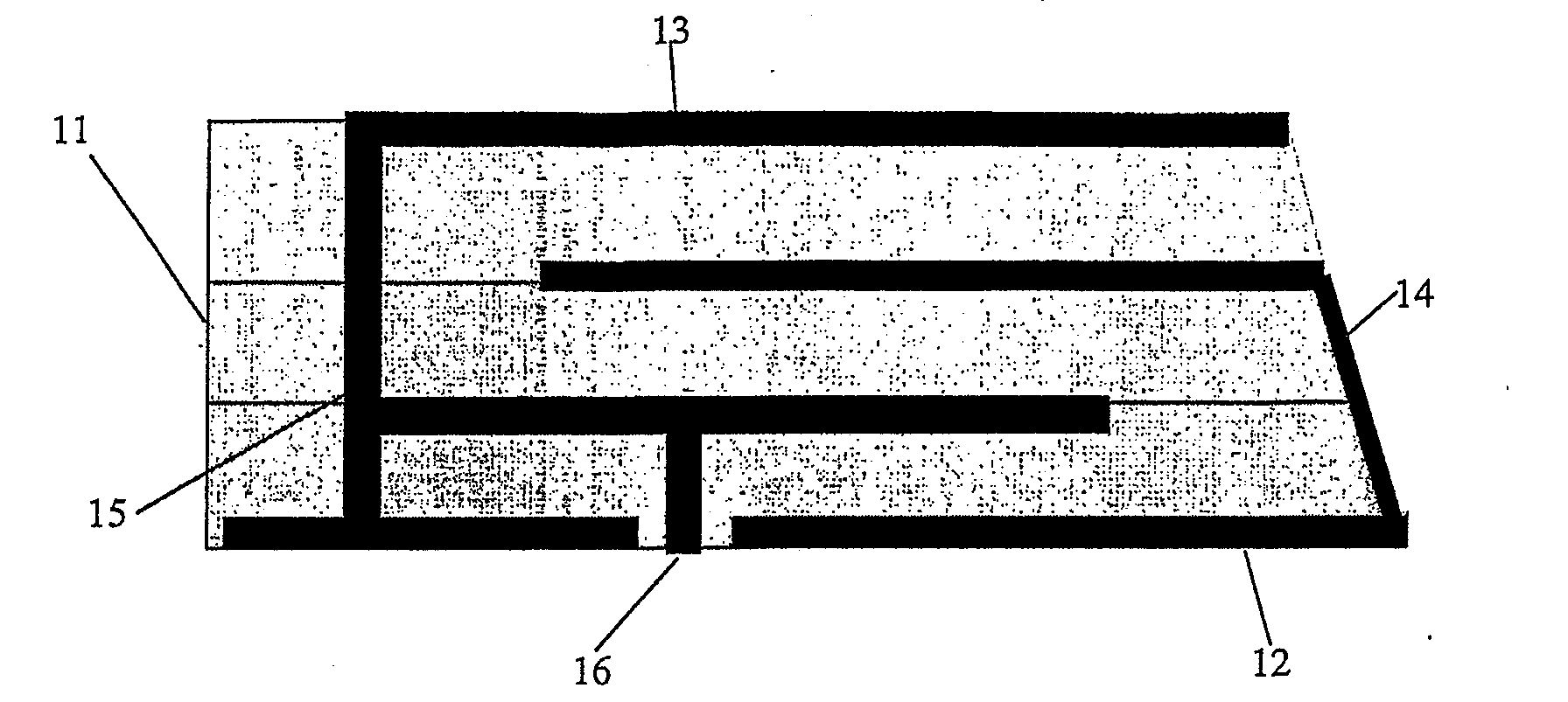
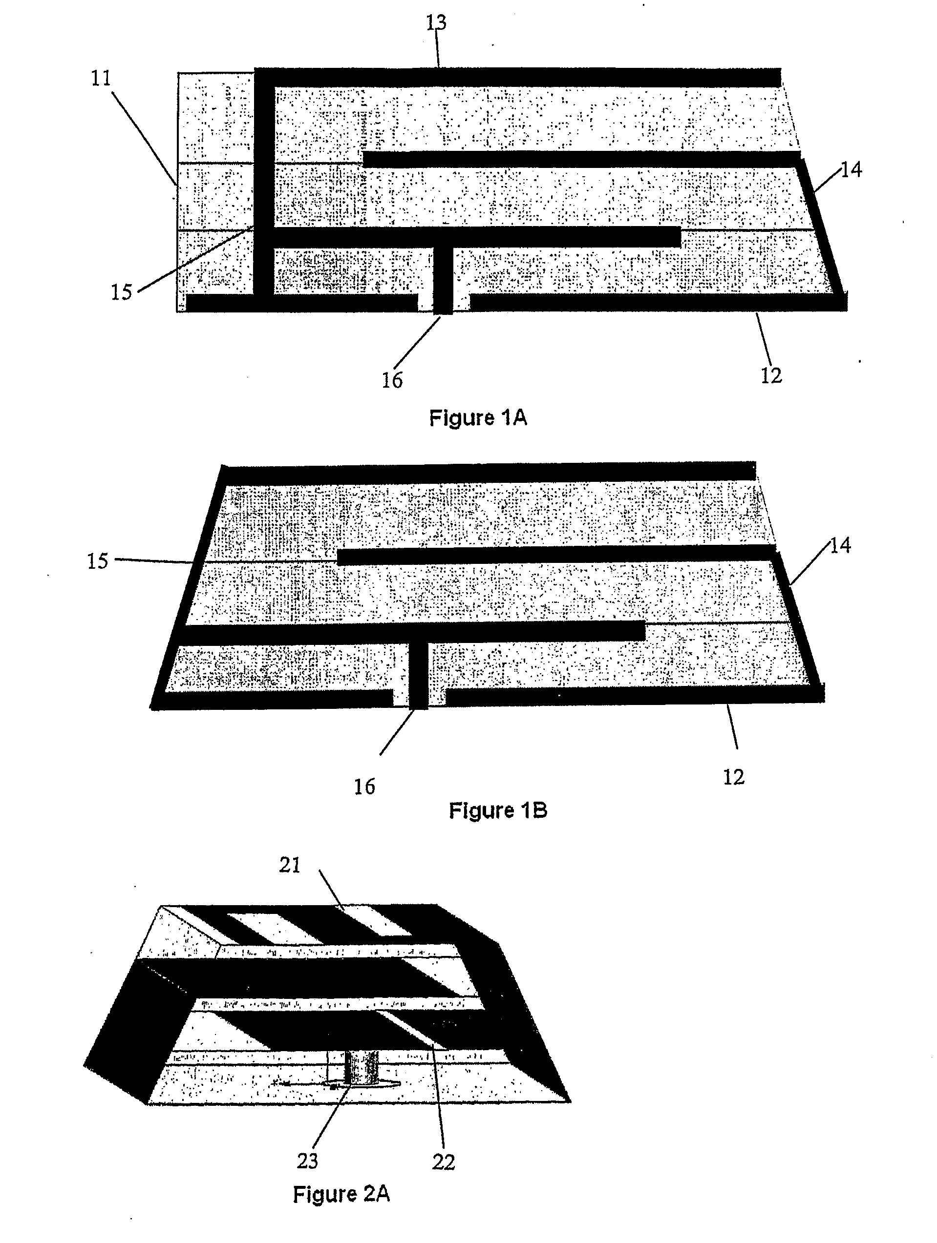
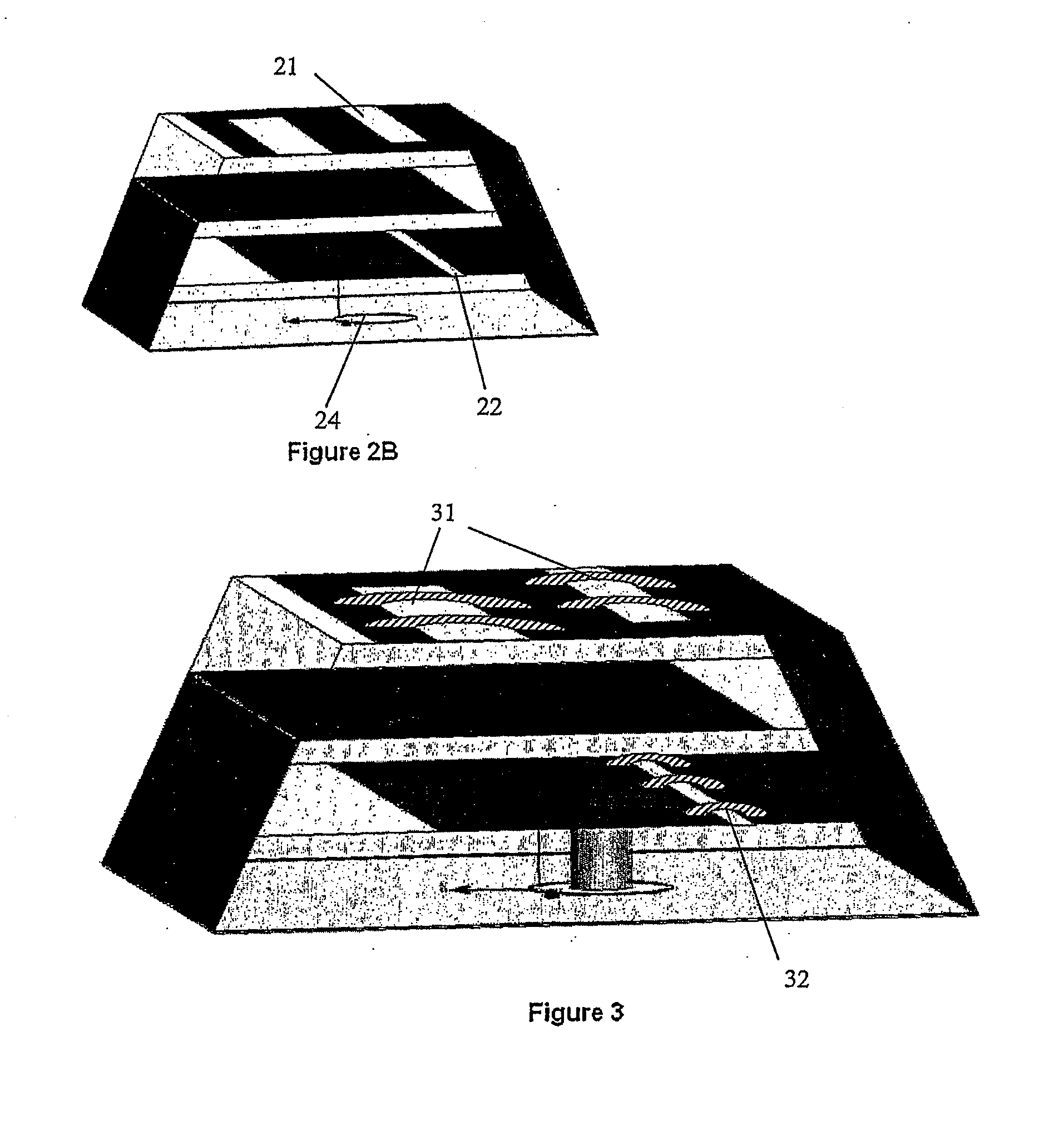
[0037]Next, the preferred embodiments of the present invention will be completely described, with reference to the appended drawings. A way to understand the preferred embodiments of the invention include their observation in the context of wireless communication devices and more specifically in the context of antennas for microsystems. However, it should be pointed out that the preferred embodiments also apply to different contexts, such as its application in mobile phones, monitoring sensors and wireless smart cards, within other related examples using antennas for send / receive data through a medium.

[0038]Next will be described a structure for the micro-antenna that can be used in a device for personal communications. A method to manufacture the micro-antenna, compatible with the process used for IC manufacturing, will be described, as well as how the slots, allowing the antenna dimension reduction, are inserted as well as how to adjust its input impedance. It will also be describ...


PUM

PropertyMeasurementUnit
Frequencyaaaaaaaaaa
Frequencyaaaaaaaaaa
Lengthaaaaaaaaaa

Abstract

The present invention describes a tunable micro-antenna of reduced electrical dimensions. This antenna consists of the agglutination of several substrate layers (11), identical or distinct, with electrical, thermal and mechanical properties compatible with the manufacturing processes of integrated circuits. These layers are interleaved with metallic sheets (12) that are interconnected by metallized walls or vias, in such a way that they form a radiating structure (15) and a ground plane (14). The radiating structure includes slots in one or more levels, therefore allowing a greater reduction of the antennas' electrical length. These slots may include switches, used to render the antenna tunable. Since the entire manufacturing method is compatible with the wafer level packaging technology, the micro-antenna is easily integrable in microsystems requiring wireless communication

Description

CROSS REFERENCE TO RELATED APPLICATIONS[0001]This application is a Continuation of International Application No. PCT / IB2006 / 052190 filed on Jun. 29, 2006, claiming priority based on Portuguese Patent Application No. 103299, filed Jun. 29, 2005, the contents of a of which are incorporated herein by reference in their entirety.SCOPE OF THE INVENTION[0002]The present invention is generically related to the field of microsystems with wireless communication, and particularly with integrated micro-antennas for wireless Microsystems.STATE OF THE ART[0003]The availability of several small personal wireless communicating devices and their potential for large-scale utilization, has been taking them to an exponential grow of popularity. This is happening especially in handheld wireless devices, such as mobile phones or in integrated circuits for Bluetooth, where an integrated antenna is usually desired. The wireless sensor network is another new emerging technology, where a high number of sm d...

Claims


Application Information

Patent Timeline
IPC IPC(8): H01Q9/04H01P11/00
CPCH01Q1/38Y10T29/49016H01Q9/0442H01Q9/0414
Inventor MATEUS MENDES, PAULOGOMES CORREIA, JOSE HIGINO
Owner UNIVERSITY OF MINHO
Why Eureka
Try Eureka