Method and Apparatus to Monitor Circuit Variation Effects on Electrically Programmable Fuses

a technology of circuit variation and fuses, applied in the field of one-time programmable memory monitor banks, can solve the problems of increasing the difficulty of sense that an efuse has been successfully blown, chip manufacturing imperfectly, and unusable portions of the chip, and achieve the effect of easy blowing and difficult blowing

Inactive Publication Date: 2008-07-03
IBM CORP
View PDF9 Cites 6 Cited by
  • Summary
  • Abstract
  • Description
  • Claims
  • Application Information

AI Technical Summary

Benefits of technology

[0012]An exemplary embodiment of the first aspect of the invention includes a monitor bank consisting of test eFuse circuits representing functional eFuse circuits (i.e. the monitor bank of test eFuses portrays, depicts, and presents the likeness of the functional eFuse circuits). The test eFuse circuits are programmed distinctively (i.e. at separate time instances) from the functional eFuse circuits. The monitor bank of test eFuse circuits is utilized to determine whether the functional eFuse circuits have been or will be reliably programmed. Within each monitor bank there may be a first eFuse circuit configured to never blow when the monitor bank is programmed, a second eFuse circuit configured to always blow when the monitor bank is programmed, and a third eFuse circuit configured to be more difficult to blow than the first eFuse circuit, but easier to blow than the second eFuse circuit.

Problems solved by technology

For a second example, sometimes chips are manufactured imperfectly and portions of the chip are unusable.
In many applications, the eFuse is blown even after an electronic system utilizing the chip has been in operation for some time.
Normal process and / or manufacturing variations in device components utilized in eFuse circuits may increase the difficulty to sense that an eFuse has been successfully blown.
Wear out mechanisms common in silicon devices can also add variability to device characteristics over time, making the ability to blow and sense eFuses difficult.
These variations have, in previous electronic systems having eFuses, resulted in eFuses failing to blow, causing logic and other design faults.
eFuses are subjected to natural or environmental component degradations, tolerances, or errors that cause the ability to blow and sense eFuses difficult.

Method used


Image

  • Method and Apparatus to Monitor Circuit Variation Effects on Electrically Programmable Fuses
  • Method and Apparatus to Monitor Circuit Variation Effects on Electrically Programmable Fuses
  • Method and Apparatus to Monitor Circuit Variation Effects on Electrically Programmable Fuses

Examples


embodiment 200

[0050]Referring now to FIG. 3, an eFuse circuit 200 is described. eFuse circuit 200 consists of sense circuitry 201, blow circuitry 204, eFuse link 202, reference resistor 203, source FS 98, NFETs 234 and 235, and ground 237. Blow circuitry 204 is supplied by voltage supply VGATE which for the purposes of embodiment 200 is the same magnitude as Vdd, the voltage supply for sense circuitry 201. In other embodiments however, VGATE and Vdd may be different magnitudes. The process of blowing eFuse link 202 is provided by waveform diagram 300 in FIG. 4, and herein described. In window 1, of FIG. 4, source FS 98 is brought high and held. In window 2, of FIG. 4, the state of FUSE SOLUTION is determined and held. The BLOW FUSE signal begins to rise toward the end of window 2. In window 3, of FIG. 4, BLOW FUSE is held high. If FUSE SOLUTION is also high, NAND gate 230 will output a ‘0’. The ‘0’ is then inverted to a ‘1’ by inverter 231 and passed to NFETs 232 and 233. Upon receipt of a ‘1’, N...

first embodiment

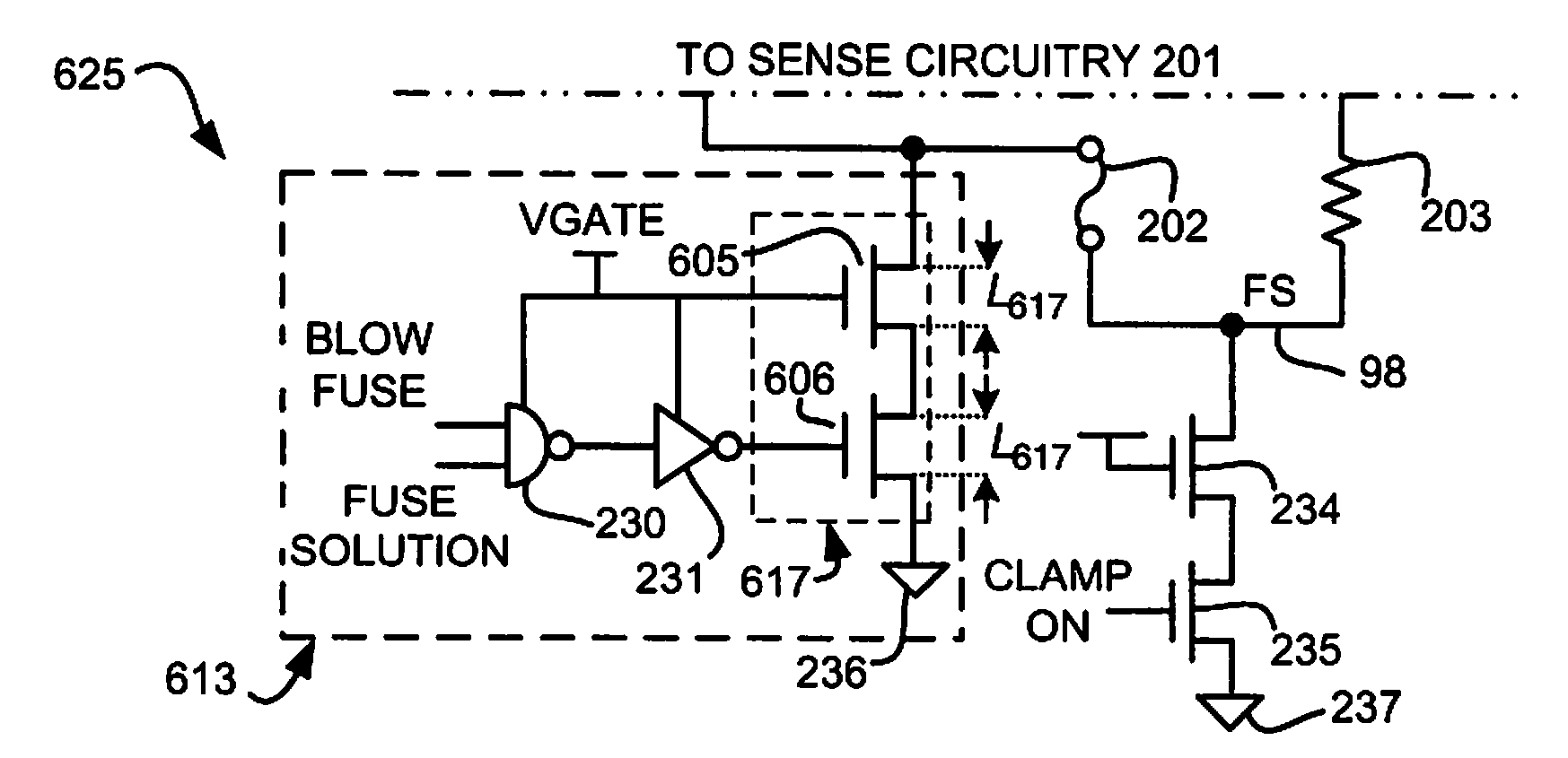
[0056]Referring now to FIGS. 6A, 6B, and 6C the invention is depicted. FIGS. 6A, 6B, and 6C depict eFuse circuits 614, 620, and 625 respectively, each eFuse circuit having blow circuitry 611, 612, and 613 respectively. eFuse circuits 614, 620, and 625 depict particular examples of eFuse circuits that are contained within a monitor bank 621 described in detail below.

[0057]Blow circuitry 611 utilizes channel length varied transistors 615, as shown as individual NFETs 601 and 602. Blow circuitry 612 utilizes channel length varied transistors 616, as shown as individual NFETs 603 and 604. Blow circuitry 613 utilizes channel length varied transistors 617, as shown as individual NFETs 605 and 606. NFETs 601 and 602 have a channel length L615, NFETs 603 and 604 have a channel length L616, and NFETs 605 and 606 have a channel length L617. Channel length L615 is less than channel length L616 which is less than channel length L617. The amount of current that travels through a transistor is in...

second embodiment

[0059]Referring now to FIG. 7A the invention is depicted. Monitor bank 621 contains a plurality of eFuse circuits 614, 620, 625, 630, and 635, herein collectively referred to as test eFuse circuits. For simplicity only channel length varied transistors 615, 616, 617, 618, and 619 are shown. eFuse circuits 630 and 635 are similar to eFuse circuits 614, 620 and 625. However eFuse circuits 630 and 635 utilize channel length varied transistors 618 and 619 respectively. Channel length varied transistors 618 are shown as NFET transistors 607 and 608 each having a channel length L618. Channel length varied transistors 619 are shown as NFET transistors 609 and 610 each having a channel length L619.

[0060]The test eFuse circuits contained in monitor bank 621 represent functional eFuse circuits (i.e. the monitor bank of test eFuses portrays, depicts, and presents the likeness of the functional eFuse circuits), and are programmed distinctively (i.e. at separate time instances) from the function...


PUM


Abstract

A monitor bank consists of test one time programmable memory that is programmed distinctively from functional one time programmable memory in order to determine whether the functional one time programmable memory has or will program successfully. In a specific embodiment, each monitor bank consists of a first eFuse configured to expectedly never blow, a second eFuse configured to expectedly always blow, and at least a third eFuse configured to be more difficult to blow than the first eFuse, but easier to blow than the second eFuse. The method of determining whether functional eFuses have or will be programmed successfully is described: programming a monitor bank; sensing whether the test eFuses have blown; creating a monitor bank bit line blow pattern; determining an anticipated bit line blow pattern; comparing the two patterns; and determining that the functional eFuses will not blow successfully if the patterns do not match.

Description

BACKGROUND OF THE INVENTION[0001]1. Field of the Invention[0002]This invention relates generally to one time programmable memories (eFuses (electrically programmable fuses), EPROM (Erasable Programmable Read-Only Memory) circuits, etc.). More specifically, this invention relates to an one time programmable memory monitor bank consisting of a plurality of test one time programmable circuits, each circuit having varying parameters, selected from a plurality of possible parameters, and utilized to evaluate whether functional one time programmable memory have or will program (i.e. blow) successfully.[0003]2. Description of the Related Art[0004]Electronic systems increasingly require function to be enabled, disabled, or modified after semiconductor chips used in the electronic systems have been manufactured or have been placed into commerce. For example, a common chip may be designed to serve multiple applications, the chip originally having circuitry to support all of the multiple appli...

Claims


Application Information

Patent Timeline
Patent Type & Authority Applications(United States)
IPC IPC(8): G11C17/16G11C17/00
CPCG11C17/18
Inventor ALLEN, DAVID H.PAONE, PHIL C. F.UHLMANN, GREGORY J.
Owner IBM CORP
Why Eureka
Try Eureka