Operating method of p-channel non-volatile memory

a non-volatile memory and operating method technology, applied in the field of memory and operating method thereof, can solve the problems of poor energy utilization, large storage capacity per unit weight, and small channel current of n-channel non-volatile memory, and achieve the effects of low power consumption, high storage capacity, and high operating speed

Inactive Publication Date: 2008-07-03
EMEMORY TECH INC
View PDF3 Cites 0 Cited by
  • Summary
  • Abstract
  • Description
  • Claims
  • Application Information

AI Technical Summary

Benefits of technology

[0009]Accordingly, at least one objective of the present invention is to provide a P-channel non-volatile memory and operating method thereof, wherein the P-channel non-volatile memory consumes lower power, has higher operating speed and higher storage capacity.
[0010]At least another objective of the present invention is to provide a P-channel non-volatile memory, wherein an additional select transistor is not required for preventing over-erasing problem.
[0019]The foregoing P-channel non-volatile memory has a low operating voltage, a low power rating, and a fast operating speed. In addition, there is no need for installing a MOS transistor, which has no storage capacity, to serve as a select transistor. Thus, the dimension of each memory cell can be substantially reduced and the level of device integration can be significantly increased.
[0021]For programming the first memory cell of the P-channel non-volatile memory, a first voltage is applied to the first doped region of the first memory cell; a second voltage is applied to the gate of the first memory cell; a third voltage is applied to the gate of the second memory cell, the channel underneath the second memory cell is turned on; a fourth voltage is applied to the third doped region of the second memory cell; and a fifth voltage is applied to the N-well. The fourth voltage is higher than the first voltage and the fourth voltage is higher than the second voltage so that the channel hot holes can induce a hot electron injection effect to program the first memory cell.
[0028]According to an embodiment of the present invention, every pair of serially connected neighboring memory cells forms a memory unit. When one of the memory cells is being operated, the other memory cell serves as a select transistor for controlling the switching of the underlying channel to prevent the operating memory cell from having program disturbance problem. Furthermore, the programming operation is carried out using the channel hot hole induced hot electron mechanism and the erasing action is carried out through the F-N tunneling effect. As a result, the operating efficiency of the P-channel non-volatile memory is enhanced.
[0029]The P-channel non-volatile memory has the advantages of a lower operating voltage, a low power rating and a fast writing speed. Furthermore, program disturbance problem can be prevented without requiring any additional select transistor. In addition, the single polysilicon structure can combine with the system-on-chip (SOC) technique in the CMOS fabrication process as well.

Problems solved by technology

Moreover, the access speed is fast, the storage capacity per unit weight is large and the access device occupies only a small volume.
The N-channel non-volatile memory has small channel current and poor energy utilization.
Therefore, in a low energy consumption portable electronic product area, the applications of an N-channel non-volatile memory is rather restricted.
If the memory cell further incorporates a select transistor, the dimension of the device will increase and accordingly limit the development of a higher level of integration for the devices.

Method used


Image

  • Operating method of p-channel non-volatile memory
  • Operating method of p-channel non-volatile memory
  • Operating method of p-channel non-volatile memory

Examples


Embodiment Construction

[0036]Reference will now be made in detail to the present preferred embodiments of the invention, examples of which are illustrated in the accompanying drawings. Wherever possible, the same reference numbers are used in the drawings and the description to refer to the same or like parts.

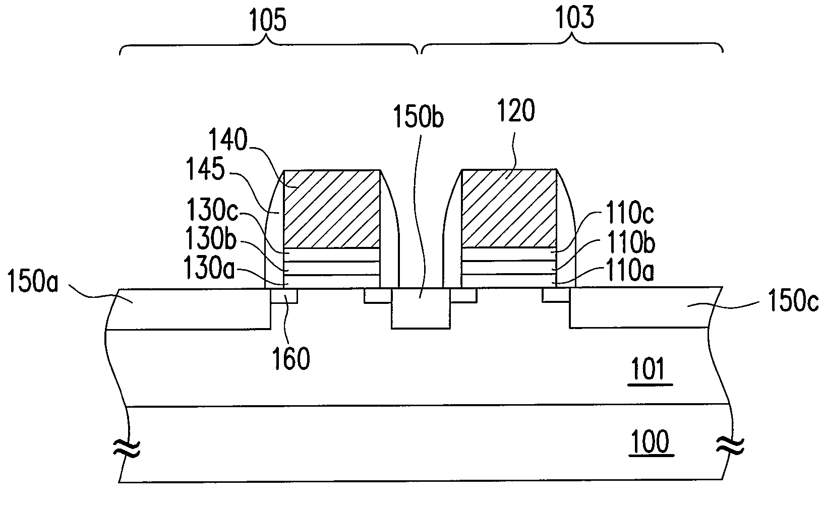
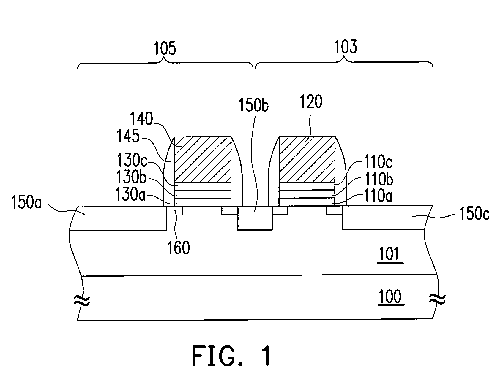
[0037]FIG. 1 is a schematic cross-sectional view of a P-channel non-volatile memory according to one embodiment of the present invention. As shown in FIG. 1, the P-channel non-volatile memory includes a substrate 100, a well 101, a first memory cell 103 and a second memory cell 105, for example. The substrate 100 is a P-type substrate, for example. The well 101 is an N-well disposed in the substrate, for example. The first memory cell 103 and the second memory cell 105 are disposed over the well 101 and are serially connected together, for example.

[0038]The first memory cell 103 includes a tunneling dielectric layer 110a, a charge storage structure 110b, a barrier dielectric layer 110c, a gate 120, a...


PUM


Abstract

A P-channel non-volatile memory is described. The P-channel non-volatile memory includes a substrate, a first memory cell, and second memory cell. An N-well is disposed over the substrate, and the first cell and the second cell are disposed over the N-well. The first memory cell includes a first gate, a first charge storage structure, a first doped region and a second doped region. The first doped region and the second doped region are disposed in the substrate on the respective sides of the first gate. The second cell includes a second gate, a second charge storage structure, a third doped region, and the second doped region. The third doped region and the second doped region are disposed in the substrate on the respective sides of the second gate. The second cell and the first cell share the second doped region.

Description

CROSS-REFERENCE TO RELATED APPLICATION[0001]This application is a divisional of an application Ser. No. 11 / 307,472, filed on Feb. 9, 2006, now pending. The entirety of the above-mentioned patent application is hereby incorporated by reference herein and made a part of this specification.BACKGROUND OF THE INVENTION[0002]1. Field of the Invention[0003]The present invention relates to a memory and operating method thereof. More particularly, the present invention relates to a P-channel non-volatile memory and operating method thereof.[0004]2. Description of the Related Art[0005]Electrically erasable programmable read-only-memory (EEPROM) is a type of non-volatile memory that allows multiple data entry, reading and erasing operations. The stored data will be retained even after power to the device is removed. Moreover, the access speed is fast, the storage capacity per unit weight is large and the access device occupies only a small volume. With these advantages, EEPROM has become one o...

Claims


Application Information

Patent Timeline
Patent Type & Authority Applications(United States)
IPC IPC(8): G11C11/34
CPCH01L27/115
Inventor LIN, YEN-TAI
Owner EMEMORY TECH INC
Why Eureka
Try Eureka