Method for chip to package interconnect

a technology of interconnection and packaging, applied in the direction of electrical equipment, basic electric elements, semiconductor devices, etc., can solve the problem of limited use of the chip, achieve the effect of saving a lithography level, improving em resistance, and simplifying the forming process

Inactive Publication Date: 2008-07-03
IBM CORP
View PDF13 Cites 8 Cited by
  • Summary
  • Abstract
  • Description
  • Claims
  • Application Information

AI Technical Summary

Benefits of technology

[0008]The present invention uses a damascene process to form a C4 element in place of the conventional plating technique. Accordingly, selection of the C4 metal is not constrained by the electrochemistry of plating (e.g., the present invention may use additional eutectic alloys). Specifically, the present invention may use lead-free, Sn-based systems such as SnAgCu, SnCu and SnZn (drop-in for SnPb eutectic alloys becaus

Problems solved by technology

The problem with the conventional process is that its use is limited to tho

Method used


Image

  • Method for chip to package interconnect
  • Method for chip to package interconnect
  • Method for chip to package interconnect

Examples


Embodiment Construction

[0012]Referring now to the drawings, and more particularly to FIGS. 2-8, there are shown exemplary embodiments of the method and structures according to the present invention.

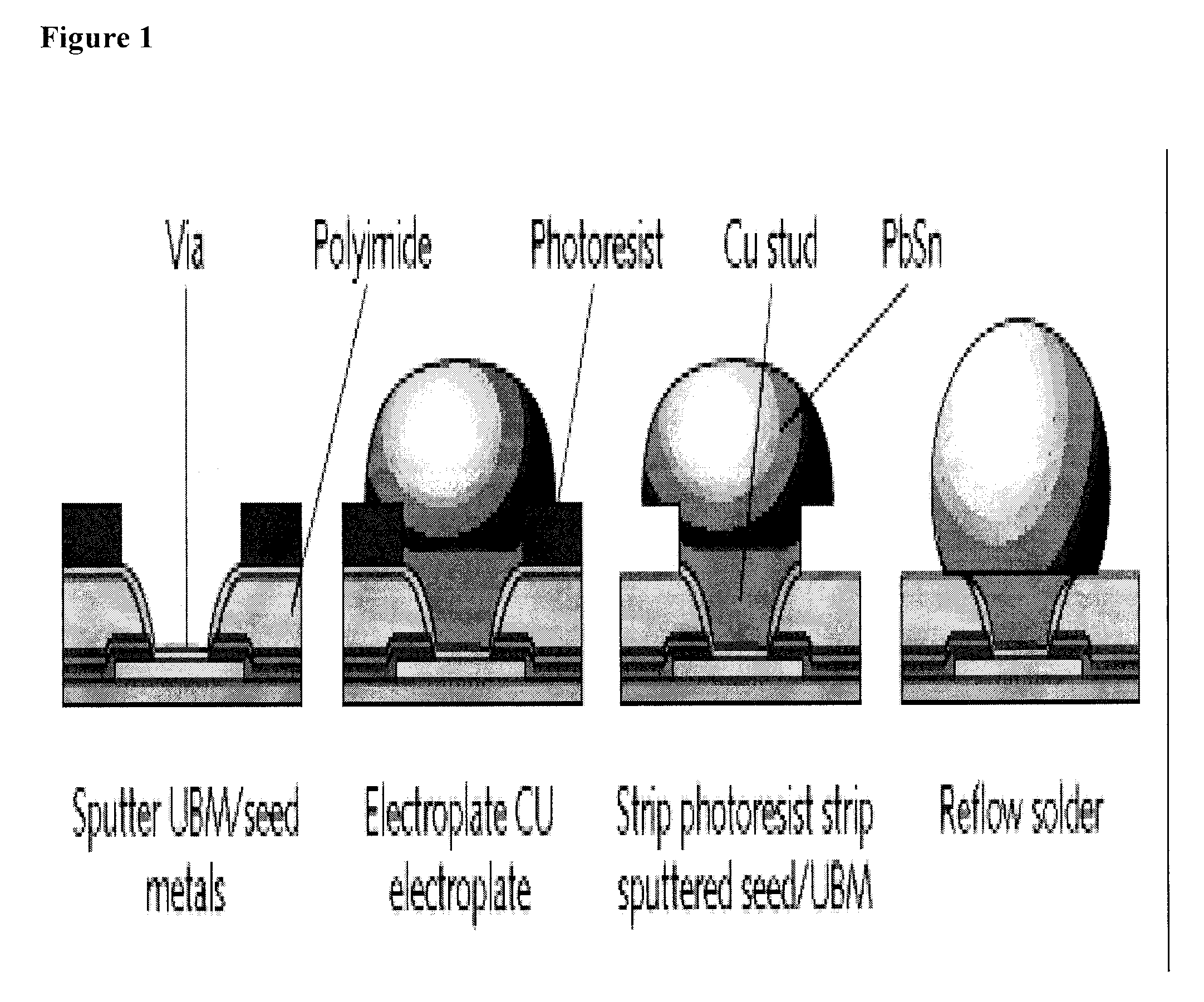
[0013]FIGS. 2-8 illustrate a method for the formation of a chip-to-package interconnect. In place of the conventional plating technique, a damascene process is used to form a C4 element. Accordingly, selection of C4 metal is not constrained by the electrochemistry of plating.

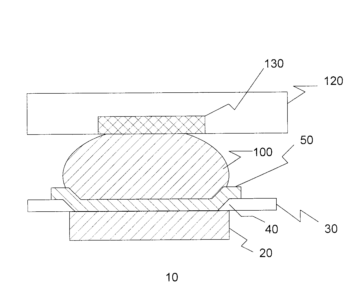
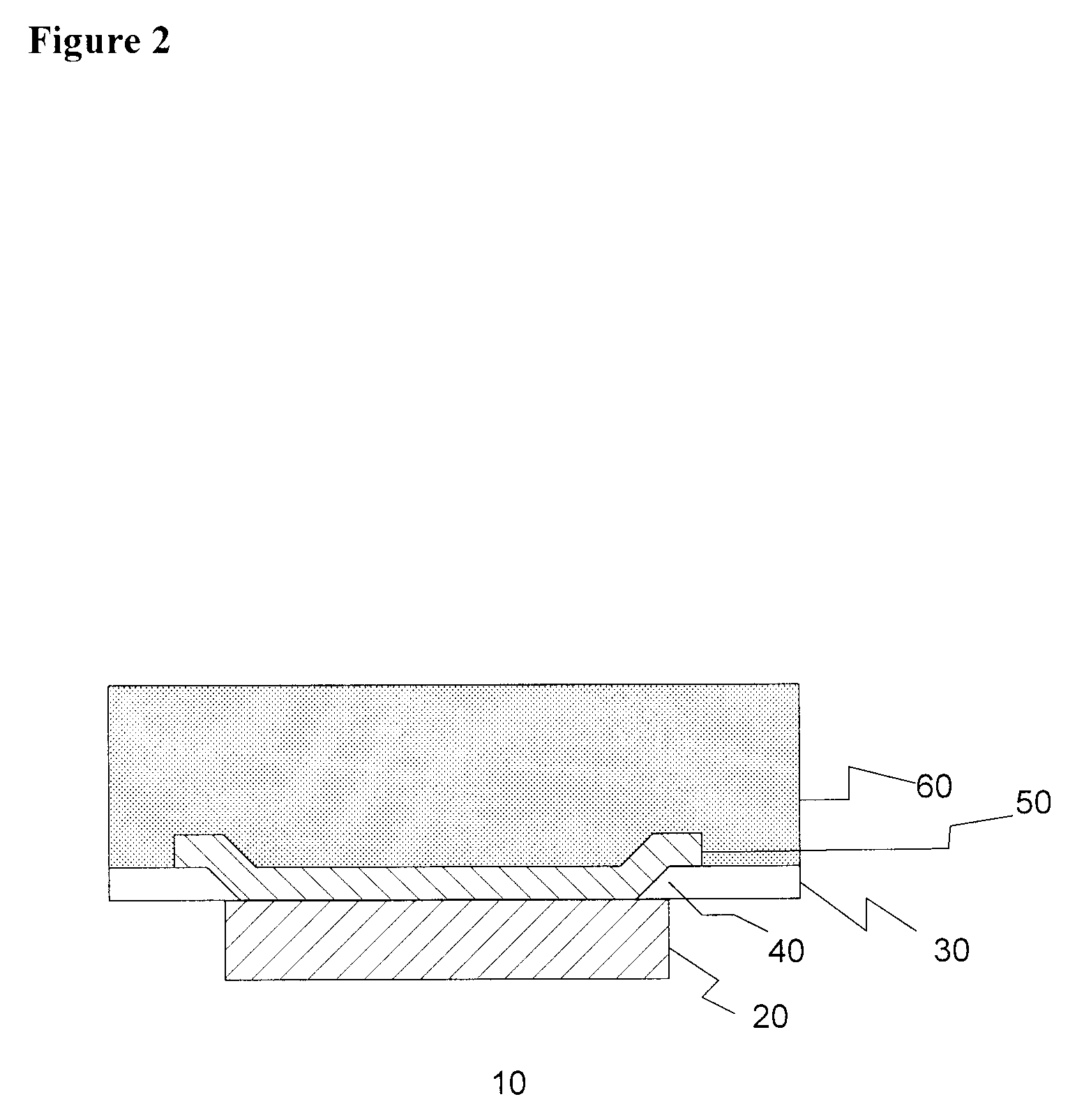
[0014]As illustrated in FIG. 2, a last level metal, or last level of copper to be deposited, 20 is formed on a substrate 10. A TV (hard passivation) ILD (Inter Level Dielectric) 40 is formed on the last level metal 20. A UBM adhesion layer 50 is lithographically patterned on the TV ILD layer 40. The UBM adhesion layer 50 may include a material selected from Ti, TiW and / or CrCu and / or Cu and / or Ni. A mandrel 60 is formed on the UBM adhesion layer 30.

[0015]Layer 20 is the final level of copper. It is formed by depositing copper metal in the v...


PUM


Abstract

A damascene method of forming a C4 element includes forming a last level metal layer on a substrate, forming a TV ILD layer on the last level metal layer, forming a lithographically patterned UBM adhesion layer including one of Ti, TiW, Cr and Cu, forming a mandrel layer over the UBM adhesion layer, lithographically patterning the mandrel layer to form an aperture, depositing a solder layer by one of sputtering, evaporation, physical vapor deposition, solder wave or injection molding in the aperture, planarizing the solder layer by CMP, removing the mandrel layer, reflowing the solder to ball the solder to form a ball interconnect, and joining a second substrate with an I/O pad to the ball interconnect.

Description

BACKGROUND OF THE INVENTION[0001]1. Field of the Invention[0002]The present invention relates to a method and apparatus for a controlled collapse chip connection (C4). In particular, the present invention describes a damascene process for forming a controlled collapse chip connection (C4) element.[0003]2. Description of the Related Art[0004]Current C4 (Controlled Collapse Chip Connection) methods primarily use plating to deposit the solder alloy. This may be done using a seed layer followed by a resist process, further followed by electrolytic plating. The seed layer typically contains the UBM (Under Bump Metallurgy) or part of the UBM. An example of UBM layers is a combination of TiW / CrCu / Cu deposited by sputtering. This is followed by electrolytic plating of a Sn / Pb alloy using a resist stencil. The resist defines the areas where the plating will occur. Subsequently, the resist is removed, and exposed seed layers are etched using wet or dry etching methods. The solder may then be ...

Claims


Application Information

Patent Timeline
IPC IPC(8): H01L21/44
CPCH01L24/11H01L24/13H01L2924/0001H01L2224/13111H01L2924/014H01L2924/01033H01L2924/01024H01L2924/01006H01L2924/04953H01L2924/01322H01L2924/01082H01L2924/01078H01L2924/01074H01L2924/01073H01L2924/01047H01L2924/01029H01L2224/11428H01L2224/1145H01L2224/1147H01L2224/11616H01L2224/1184H01L2224/11901H01L2224/13007H01L2224/13099H01L2924/01013H01L2924/01022H01L2924/00014H01L2924/0103H01L24/03H01L24/05H01L2224/05001H01L2224/05022H01L2224/05572H01L2224/05624H01L2224/05647H01L2224/05655H01L2224/05666H01L2224/05671H01L2224/05684H01L2224/05099
Inventor CLEVENGER, LAWRENCEDALTON, TIMOTHY J.FAROOQ, MUKTA GHATELANDERS, WILLIAM FRANCISRADENS, CARLYANG, CHIH-CHAO
Owner IBM CORP
Why Eureka
Try Eureka