
Method For Manufacturing Semiconductor Device

a manufacturing method and semiconductor technology, applied in the direction of semiconductor devices, basic electric elements, electrical appliances, etc., can solve the problems of device defects, further decrease of treatment temperature, and defect of semiconductor devices

Inactive Publication Date: 2008-07-03
IHI CORP
View PDF20 Cites 32 Cited by
  • Summary
  • Abstract
  • Description
  • Claims
  • Application Information

AI Technical Summary

Benefits of technology

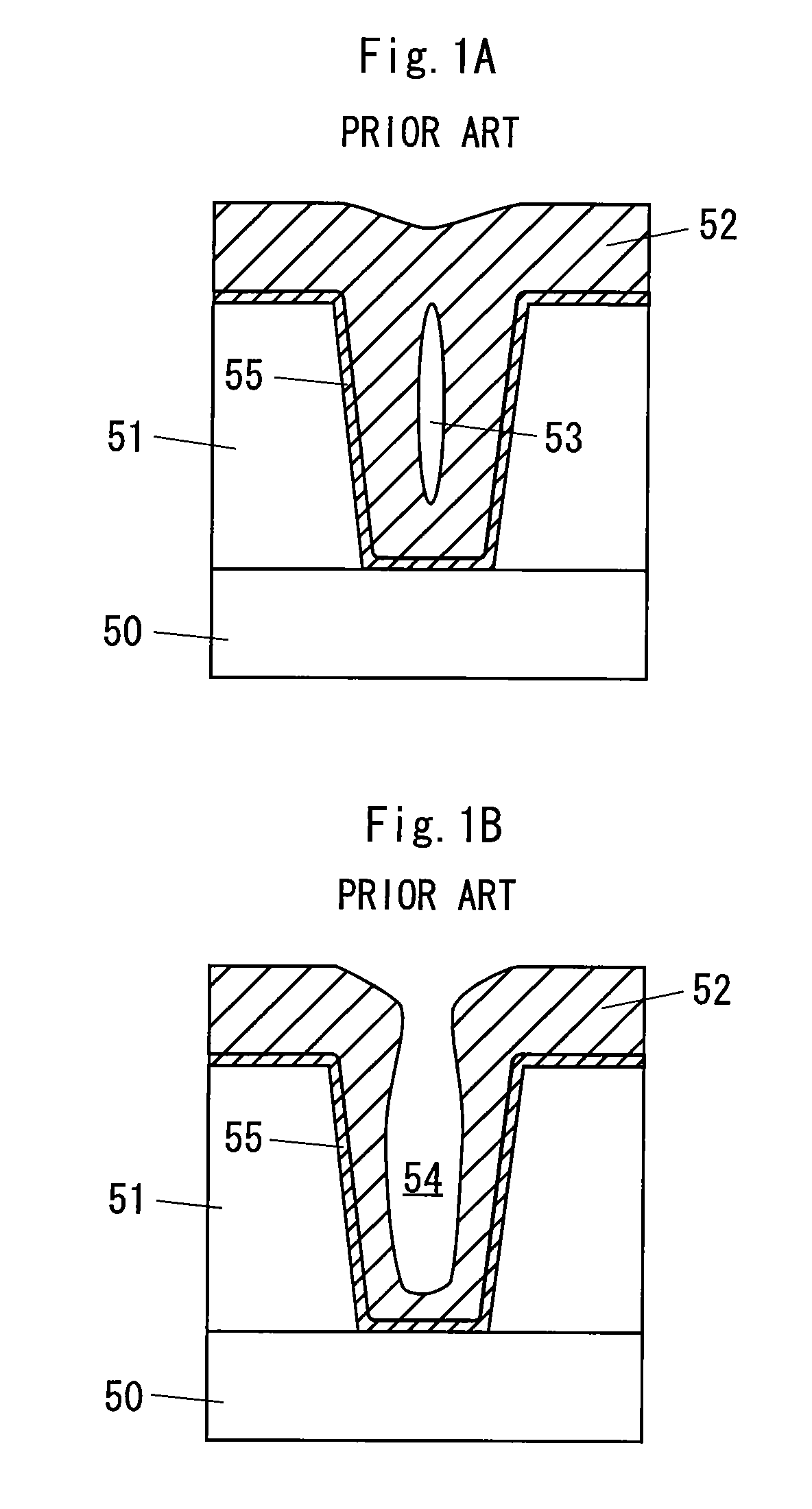
[0012]The present invention has been developed in order to solve the above problems. That is, an object of the present invention is to provide a method for manufacturing a semiconductor device, in which voids in an inter layer dielectric can completely be eliminated at a heat treatment temperature that is lower than before, and further open pores generated in the inter layer dielectric can be filled in.
[0013]To achieve the object of the present invention, according to a first aspect of the invention, there is provided a method for manufacturing semiconductor device, including: a first film forming step of forming, on a concave and convex portion formed by an element on a semiconductor substrate, an oxidation preventive layer which prevents permeation of moisture into the element; a second film forming step of forming, on this oxidation preventive layer, an expansion layer which can be oxidized and expanded by a heat treatment in an oxidation atmosphere; a third film forming step of forming, on this expansion layer, an insulating film which can be fluidized by the heat treatment in the oxidation atmosphere; and an expansion step of subjecting, to the heat treatment in the oxidation atmosphere, the semiconductor substrate on which the oxidation preventive layer, the expansion layer and the insulating film have been formed, to fluidize the insulating film and to oxidize and expand the expansion layer, thereby eliminating bubbles generated in the insulating film.

Problems solved by technology

In a case where wiring lines are formed to intersect with one another, a lap portion of an intersecting portion becomes thin, and this causes disconnection.
Such problems are generated which result in defects of the semiconductor device.
However, since the heat treatment temperature of 700° C. to 800° C. as in Patent Documents 1 and 2 adversely affects characteristics of the element to be miniaturized, there is a demand for a further decrease of the treatment temperature to reduce damages due to the heat treatment in further integrating the semiconductor device.
The remaining voids might cause a device defect.
Especially as the size of the voids is decreased, an effect produced by buoyancy during the fluidization deteriorates, and this increasingly raises a possibility that the voids remain.

Method used


Image

  • Method For Manufacturing Semiconductor Device
  • Method For Manufacturing Semiconductor Device
  • Method For Manufacturing Semiconductor Device

Examples


first embodiment

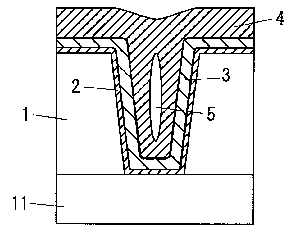
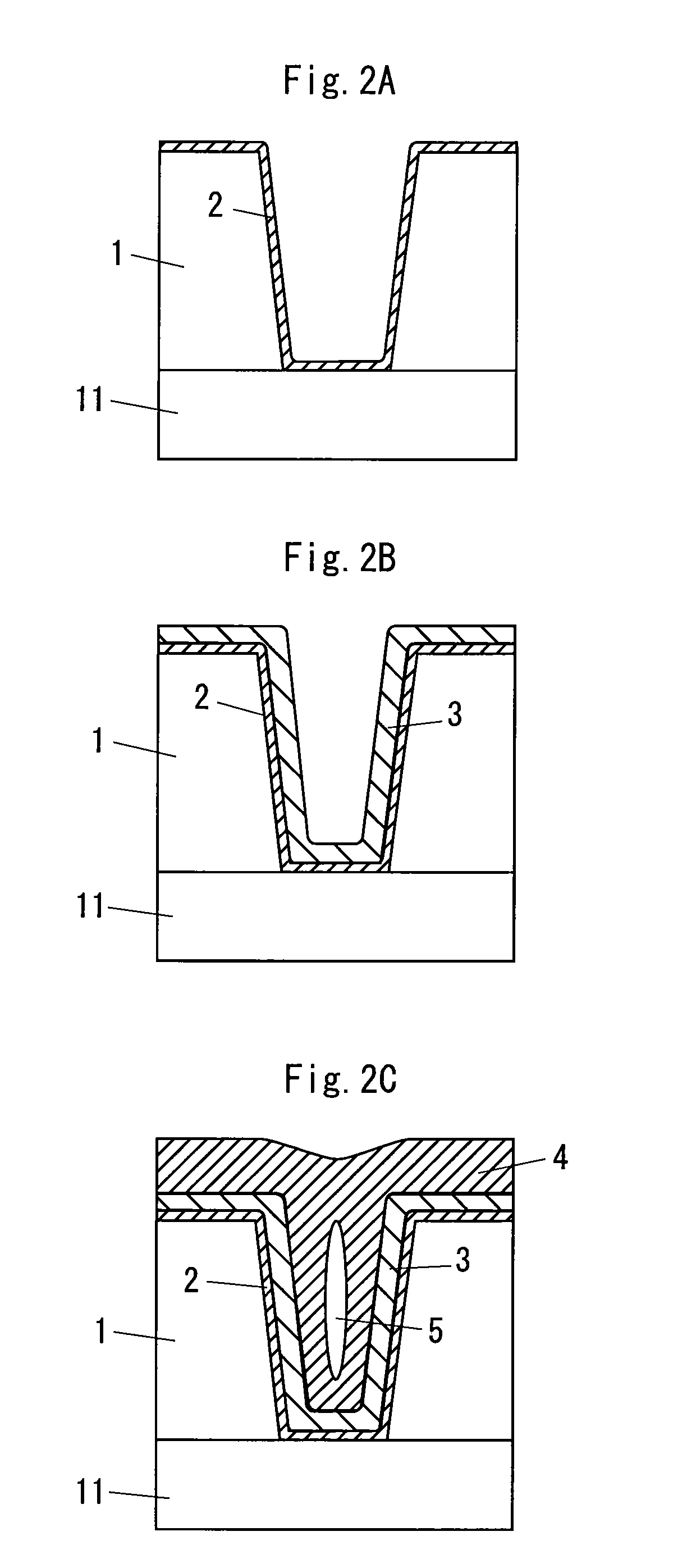
[0038]FIGS. 2A to 2C show sectional shapes of the semiconductor device to which there is applied the method for manufacturing semiconductor device in the present invention. First, as shown in FIG. 2A, the first film forming step is performed to form an oxidation preventive layer 2 as a first layer by a low-pressure chemical vapor deposition (hereinafter referred to as “LPCVD”) on a concave and convex portion 1 (trench) formed by a wiring structure (element) such as a gate insulating film or a gate electrode formed on a semiconductor substrate 11. In the present embodiment, a magnitude of the trench of the concave and convex portion 1 indicates a width of 1 μm and a depth of 2.5 μm, and the oxidation preventive layer 2 having a thickness of 150 nm was formed on this portion. This oxidation preventive layer 2 is formed of, for example, a silicon nitride film, and functions as a protective film (barrier layer) for preventing permeation of moisture due to a treatment of the subsequent s...

second embodiment

[0055]As described above, according to the method for manufacturing semiconductor device in the present invention, the oxidation preventive layer 2 is formed on the concave and convex portion 1 formed by the element on the semiconductor substrate 11, and on the layer, the expansion flow layer 6 is formed. Moreover, the semiconductor device on which these films have been formed is subjected to the heat treatment in the high-pressure oxidation atmosphere to expand and fluidize the expansion flow layer 6, whereby it is possible to obtain an effect that the void 5 (bubble) generated in the expansion flow layer 6 can completely be eliminated. Even in a case where the open pore 7 is generated because the concave and convex portion 1 is insufficiently filled with the expansion flow layer 6, the open pore 7 is filled in owing to the effects of expansion and fluidization, whereby it is possible to obtain an effect that the open pore 7 can be eliminated. As this result, yield of the device ca...


PUM


Abstract

A method for manufacturing semiconductor device according to the present invention comprises a first film forming step of forming, on a concave and convex portion formed by an element on a semiconductor substrate, an oxidation preventive layer which prevents permeation of moisture into the element; a second film forming step of forming, on this oxidation preventive layer, an expansion layer which can be oxidized and expanded by a heat treatment in an oxidation atmosphere; a third film forming step of forming, on this expansion layer, an insulating film which can be fluidized by the heat treatment in the oxidation atmosphere; and an expansion step of subjecting, to the heat treatment in the oxidation atmosphere, the semiconductor substrate on which the oxidation preventive layer, the expansion layer and the insulating film have been formed, to fluidize the insulating film and to oxidize and expand the expansion layer, thereby eliminating bubbles generated in the insulating film.

Description

BACKGROUND OF THE INVENTION[0001]1. Technical Field of the Invention[0002]The present invention relates to a method for manufacturing a semiconductor device including an insulating film on a semiconductor substrate (wafer). More particularly, it relates to a method for manufacturing semiconductor device which can completely eliminate voids (bubbles) generated in the insulating film or open pores generated owing to insufficient filling-in of the insulating film.[0003]2. Description of the Related Art[0004]For example, in steps of manufacturing a semiconductor device, an MOSFET gate electrode is formed on a semiconductor substrate to protrude therefrom, whereby a concave portion is formed between the gate electrode and a gate electrode adjacent to the electrode, and a concave portion, a convex portion and a stepped portion (trench) are made in the gate electrode and between the gate electrodes. When this stepped portion enlarges, there occurs focus deviation during drawing of a wiring...

Claims


Application Information

Patent Timeline
IPC IPC(8): H01L21/469H01L21/316H01L21/762H01L21/768
CPCH01L21/3165H01L21/76232H01L21/76801H01L21/76837H01L2924/0002H01L2924/00H01L21/02131H01L21/02129H01L21/02255H01L21/324
Inventor WATANABE, TOMOYUKIYOSHINOUCHI, ATSUSHI
Owner IHI CORP
Learn More