Manufacturing method for integrating passive component within substrate

a manufacturing method and passive component technology, applied in the association of printed circuit non-printed electric components, conductive pattern formation, final product manufacturing, etc., can solve the problems of affecting the product yield, the position of drilling cannot be placed to the electrical contact of passive components, and the parasitic effect of electronic devices is a great problem, so as to prevent positioning errors

Active Publication Date: 2008-07-10
ADVANCED SEMICON ENG INC
View PDF9 Cites 5 Cited by
  • Summary
  • Abstract
  • Description
  • Claims
  • Application Information

AI Technical Summary

Benefits of technology

[0009]Therefore, with the application of the method disclosed in the embodiments of the present invention, the passive component can be positioned on the circuit layer and electrically connected thereto via a conductive material in the positioning blind hole before a laminating step, wherein the conductive material may be adhesive to position the passive component in advance, thereby preventing positioning error and the passive component can not electrically connect with the circuit.

Problems solved by technology

Further, for the integrity of signal, in high frequency circuit design, the parasitic effect of electronic devices is a great issue.
However, the position of drilling is predetermined, and if the position of the passive component is not accurate and precise, the position of drilling can not position to the electrical contact of the passive component.
Therefore, the electrical connection of the passive component can not be achieved, thus affecting the product's yield significantly.

Method used


Image

  • Manufacturing method for integrating passive component within substrate
  • Manufacturing method for integrating passive component within substrate
  • Manufacturing method for integrating passive component within substrate

Examples


Embodiment Construction

[0014]In order to make the illustration of the present invention more explicit and complete, the following description is stated with reference to FIG. 1A through FIG. 3.

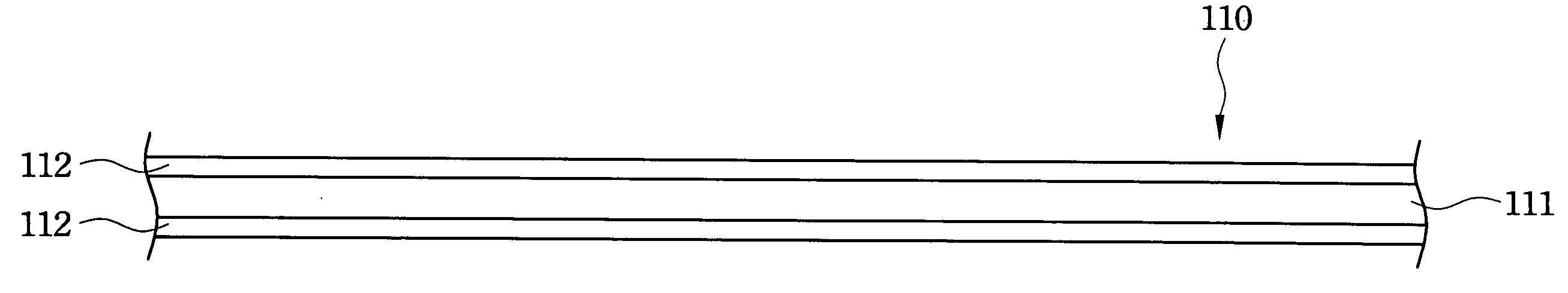
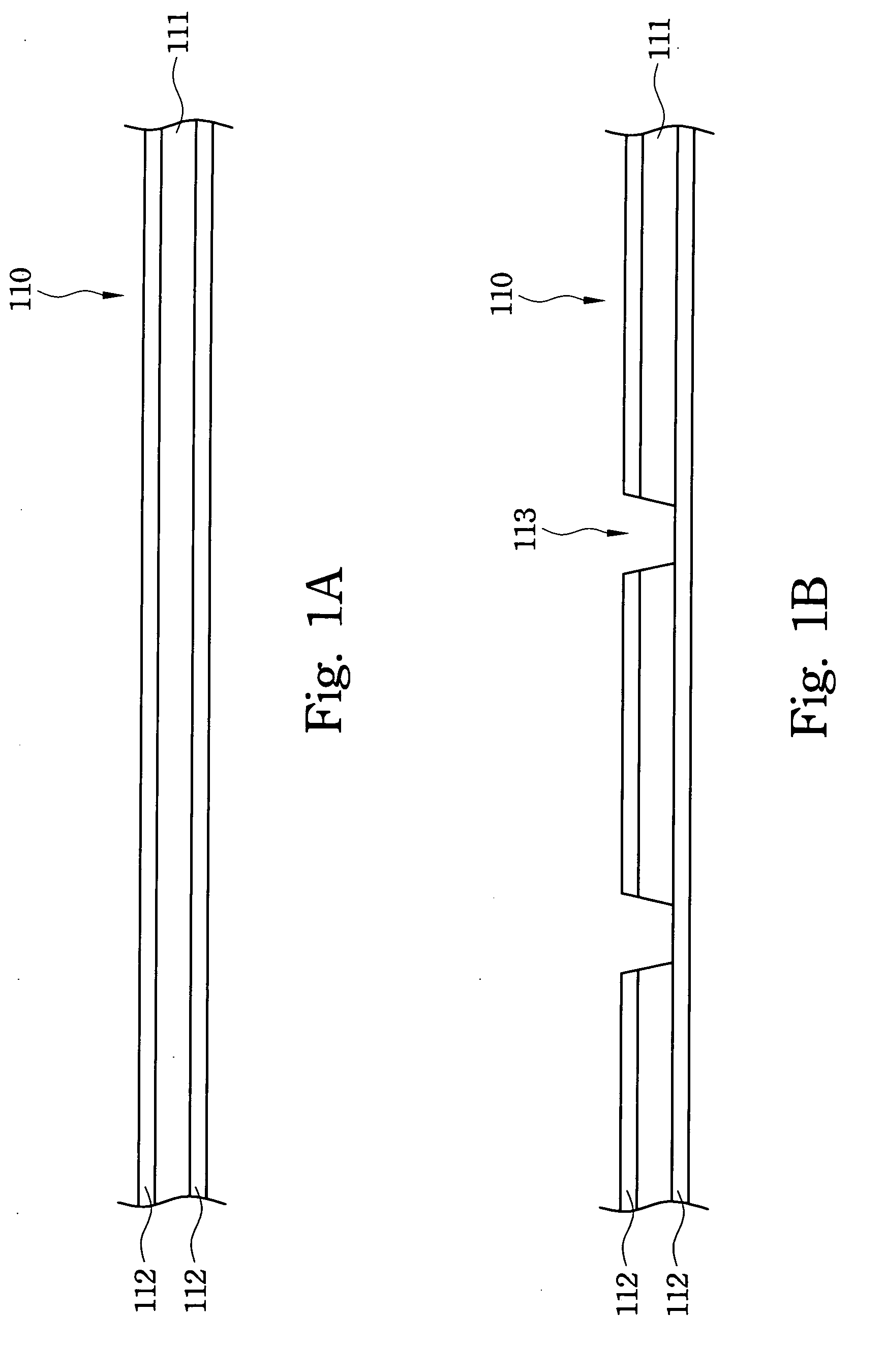
[0015]Refer to FIG. 1A through FIG. 1H. FIG. 1A through FIG. 1H are schematic flow diagrams showing the process for integrating at least one passive component within a substrate according to a first embodiment of the present invention. Refer to FIG. 1A again. First, a circuit layer 110 is provided. The circuit layer 110 includes an intermediate layer 111 and an electrically conductive layer 112. The intermediate layer 111 is made of dielectric material. The electrically conductive layer 112 is formed at both sides of the intermediate layer 111 and made of metal material, such as Cu, Ni or Au.

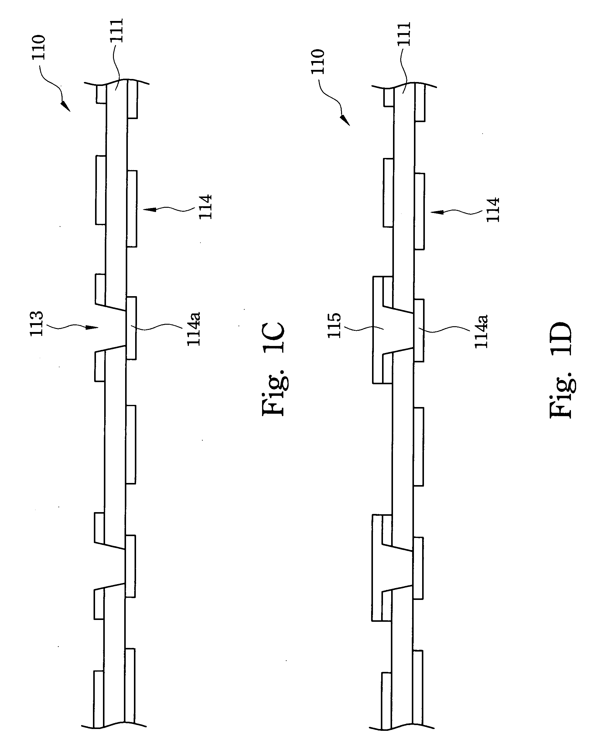
[0016]Refer to FIG. 1B again. Next, at least one positioning blind hole 113 is formed in the circuit layer 110. The positioning blind hole 113 may be formed by a method such as laser drilling or mechanical drilling. The position...


PUM

PropertyMeasurementUnit
conductiveaaaaaaaaaa
electrically conductiveaaaaaaaaaa
sizeaaaaaaaaaa

Abstract

A manufacturing method for integrating a passive component within a substrate is disclosed. The manufacturing method comprises the steps of: providing a circuit layer, wherein a positioning blind hole is formed in the circuit layer; forming a conductive material in the positioning blind hole; positioning the passive component in the positioning blind hole of the circuit layer and electrically connecting the passive component to the circuit layer via the conductive material in the positioning blind hole; and laminating a core layer, the passive component, and the circuit layer as the substrate.

Description

RELATED APPLICATIONS[0001]This application claims priority to Taiwan Application Serial Number 96100979, filed Jan. 10, 2007, which is herein incorporated by reference.FIELD OF THE INVENTION[0002]This invention relates to a manufacturing method for integrating at least one passive component within a substrate, and more particularly, to a method for positioning the passive component in the substrate in advance.BACKGROUND OF THE INVENTION[0003]For electronic devices today, the need of functionality and small size has gradually increased, and thus designers and suppliers thereof have to integrate more electronic devices into a package system. As to chip package, multi-chip module (MCM) or system-in-package (SIP) may provide the resolution of the foregoing problem. If MCM or SIP cooperated with embedding technique is used for integrating the Surface Mount Technology (SMT) passive components into a package substrate, more space on the surface of the substrate can be enhanced. Further, fo...

Claims


Application Information

Patent Timeline
Patent Type & Authority Applications(United States)
IPC IPC(8): H05K3/30H01K3/10
CPCH05K1/186Y10T29/49126H05K3/4626H05K2201/09481H05K2201/10636H05K2203/063Y10T29/49156Y10T29/49171Y10T29/49142Y10T29/49192Y10T29/4913Y10T29/49117Y10T29/49155Y10T29/49124Y10T29/49165Y10T29/49144H05K3/321Y02P70/50
Inventor WANG, CHIEN-HAO
Owner ADVANCED SEMICON ENG INC
Why Eureka
Try Eureka