High frequency signal detection circuit

Inactive Publication Date: 2008-07-17
LAPIS SEMICON CO LTD
View PDF14 Cites 12 Cited by
  • Summary
  • Abstract
  • Description
  • Claims
  • Application Information

AI Technical Summary

Benefits of technology

[0007]An objective of the invention is to solve the above-described problem and to provide a high frequency signal detection circuit, which can effectively detect a

Problems solved by technology

However, there is a problem that a high freq

Method used


Image

  • High frequency signal detection circuit
  • High frequency signal detection circuit
  • High frequency signal detection circuit

Examples


first embodiment

The First Embodiment

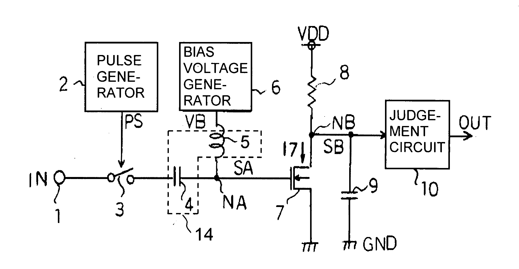
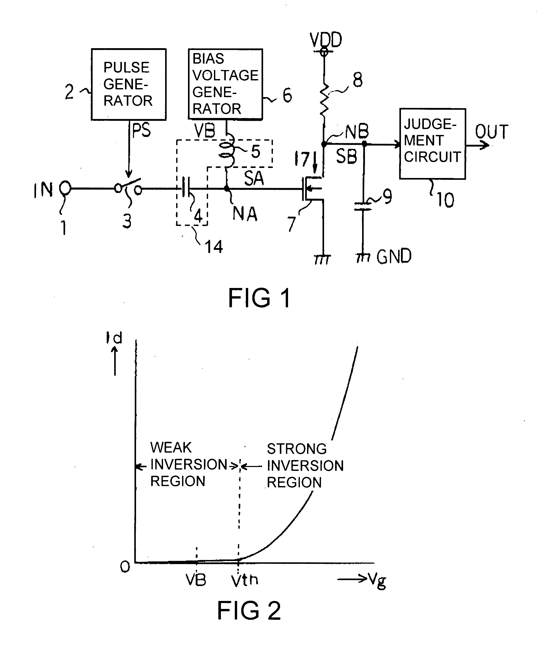
[0015]FIG. 1 is a high frequency signal detection circuit 100, according to the first

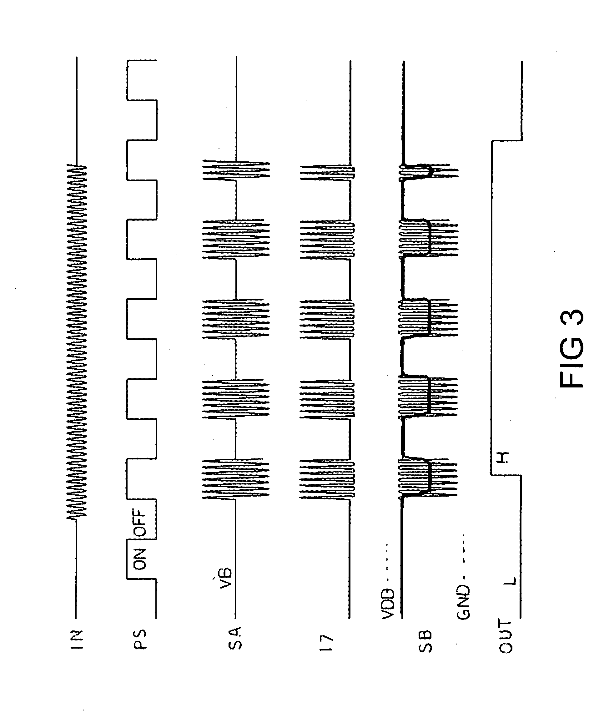
[0016]5. embodiment of the invention. The high frequency signal detection circuit 100 includes an input terminal 1 at which a high frequency signal IN with 5 GHz to be detected is applied. The input terminal 1 is connected to one end of a first capacitor 4 though a switch 3, which is on / off controlled in response to a pulse signal PS with 16 kHz, which is applied from a pulse generator 2. The other end of the first capacitor 4 is connected to a first node NA. The first node NA is connected to a bias voltage generator 6 via an inductor 5, and is connected to a gate of an N channel MOSFET (hereinafter called an NMOS).

[0017]The first capacitor 4 has a function for cutting a direct current component of the high frequency signal IN, and creates a resonant circuit 14 together with the inductor 5. The resonant circuit 14 is set to be synchronized with the frequency of the high frequency...

second embodiment

The Second Embodiment

[0032]FIG. 4 is a circuit diagram of a high frequency signal detection circuit, according to the second embodiment. In FIG. 4, the same reference numbers designate the same or similar components used in FIG. 1

[0033]Compared with the high frequency signal detection circuit 100, the high frequency signal detection circuit 200 includes a first capacitor 4 located between an input terminal IN and a switch 3, and a bias voltage generator 11 using a current-mirror circuit for controlling the bias current of a first NMOS 7. The bias voltage generator 11 includes a constant current generator 11a generating a constant electric current, which corresponds to the drain current at the operating point of the first NMOS 7, and a second NMOS 11b being connected between the constant current generator 11a and the ground GND. The output of the constant current generator 11a is connected to the drain of the second NMOS 11b, and the voltages at the gate and at the drain of the secon...


PUM


Abstract

A high frequency signal detection circuit includes an input terminal for a high frequency signal to be detected, a switch transferring the high frequency signal as intermittent ringing signal to a first node in response to a pulse signal whose frequency is lower than that of the high frequency signal, a transistor amplifying the signal at the first node, and outputting to a second node, a bias generator generating a bias voltage by which the transistor is operated in its weak inversion region, a resonant circuit outputting the bias voltage to the first node, and resonating the high frequency signal, a capacitor removing a high frequency component of the signal at the second node; and a judgment circuit judging whether or not the high frequency signal is inputted by detecting the signal at the second node, which has the same frequency as the pulse signal.

Description

CROSS-REFERENCE TO RELATED APPLICATION[0001]This application claims the priority benefit of Japanese Patent Application No. 2007-007993, filed Jan. 17, 2007, the entire disclosure of which is incorporated herein by reference.BACKGROUND OF THE INVENTION[0002]1. Field of the Invention[0003]The invention relates to a high frequency signal detection circuit used in the radio communication device, detecting a very small high frequency signal inputted from an antenna.[0004]2. Description of the Related Art[0005]Japanese patent 2,561,023 discloses a conventional high frequency signal level detection circuit. Under the '023 Japanese patent, the circuit detects a level of a high frequency signal by detecting the signal by a semiconductor diode. Under the circuit, the bias voltage for the use of the detection of the semiconductor diode is changed into three levels periodically. Then, the circuit calculates a static characteristic at that time from the diode currents over two voltages that are...

Claims


Application Information

Patent Timeline
IPC IPC(8): H03D1/18
CPCH03D1/18
Inventor TODA, HIROYUKI
Owner LAPIS SEMICON CO LTD
Why Eureka
Try Eureka