Method and apparatus for on-chip phase error measurement to determine jitter in phase-locked loops

a phase error and phase-locked loop technology, applied in the field of on-chip diagnostics and testability, can solve the problems of increasing power and area consumption, slow external diagnostic path, and increasing difficulty in predicting the behavior of transistor devices and passive elements such as resistors and capacitors

Active Publication Date: 2008-07-17
GLOBALFOUNDRIES US INC
View PDF54 Cites 43 Cited by
  • Summary
  • Abstract
  • Description
  • Claims
  • Application Information

AI Technical Summary

Problems solved by technology

As technology advances, predicting the behavior of transistor devices and passive elements such as resistors and capacitors becomes increasingly difficult.
Conservative designs may often result in more power and area consumption than is needed.
However, an external diagnostic path is slow, and solutions are not always found.
Furthermore, the limited off-chip visibility of internal analog / digital waveforms results in limited learning rates for yield.
In phase-locked loop (PLL) design, key PLL parameters such as jitter, static phase error, and control voltage range are extremely difficult to evaluate in integrated systems.
Among these, measuring jitter performance is very challenging, as timing uncertainty in clock generation increases with modern technology.
However, a large number of delay lines could induce additional jitter generation, possibly degrading jitter measurement performance.
Also, jitter measurements using an analog charge pump are not favorable due to mismatch requirements of transistors.

Method used


Image

  • Method and apparatus for on-chip phase error measurement to determine jitter in phase-locked loops
  • Method and apparatus for on-chip phase error measurement to determine jitter in phase-locked loops
  • Method and apparatus for on-chip phase error measurement to determine jitter in phase-locked loops

Examples


Embodiment Construction

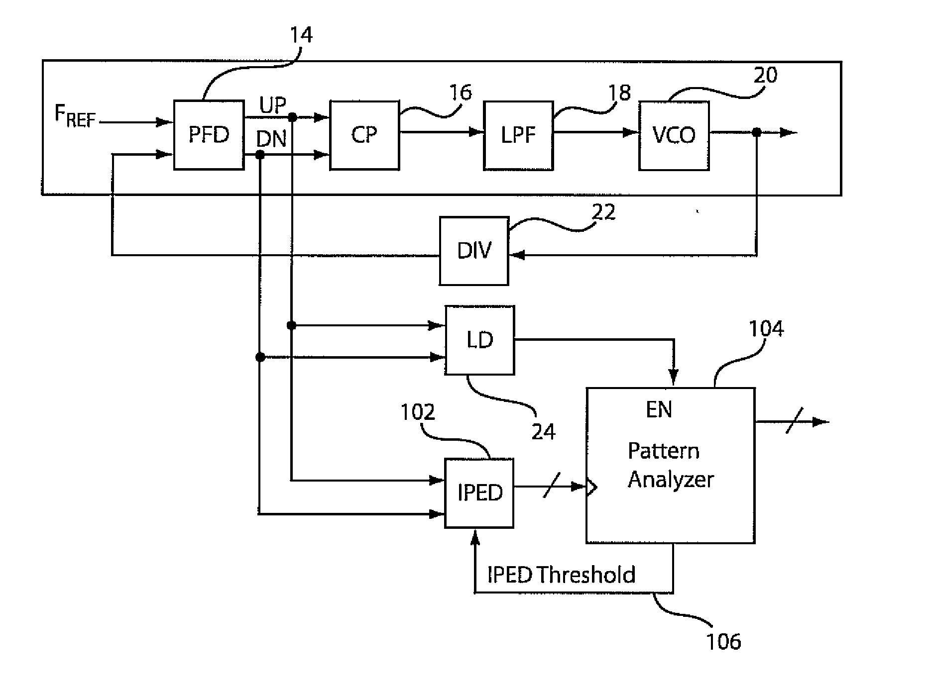
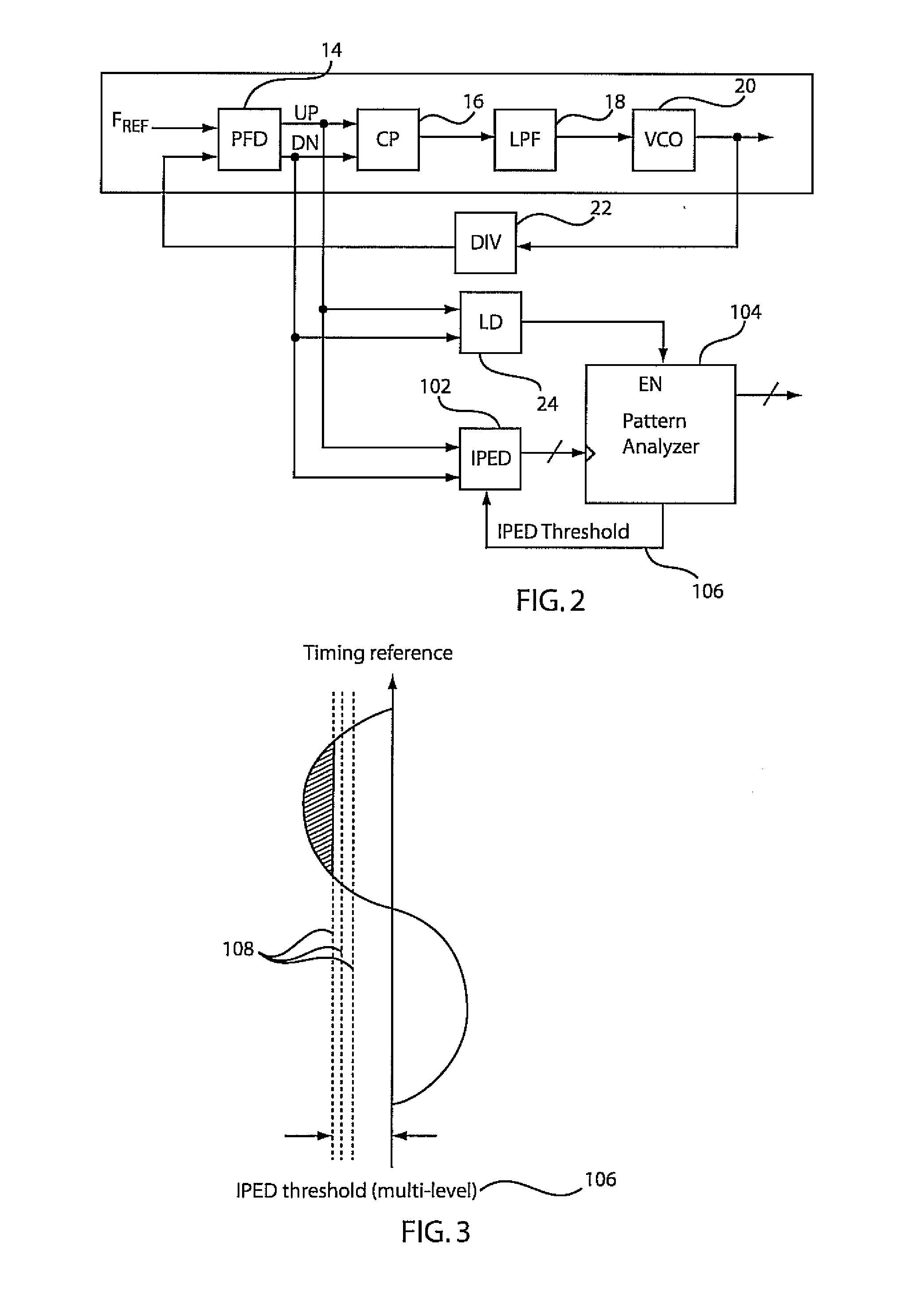
[0030]A system, apparatus and method employ phase-locked loop (PLL) circuits to simplify hardware complexity by using information already present in the PLL. A monitor circuit in accordance with present principles operates by measuring a phase error at each reference clock cycle with a programmable error-detection threshold and saves the information in latches for post processing. An all-digital peak detector may be employed, which detects peak phase error amplitude only, instead of measuring metastability in the zero-time crossing. Simple lumped delay lines are preferably employed. Hardware complexity and power consumption is reduced since phase error amplitude is detected at a phase-frequency detector (PFD) output, meaning that the monitor circuit does not need to operate at the (typically higher) VCO frequency.

[0031]Embodiments of the present invention can take the form of an entirely hardware embodiment, an entirely software embodiment or an embodiment including both hardware an...


PUM


Abstract

An apparatus includes a phase-locked loop (PLL) circuit including a phase-frequency detector configured to output phase error signals. A phase error monitor circuit is configured to determine instantaneous peak phase error by logically combining the phase error signals and comparing pulse widths of the logically combined phase error signals to a programmable delay time at each reference clock cycle to determine instantaneous phase error change. A storage element is configured to store the instantaneous phase error change.

Description

BACKGROUND[0001]1. Technical Field[0002]The present invention relates to on-chip diagnostics and testability, and in particular, to phase-locked loop circuits with jitter measurement.[0003]2. Description of the Related Art[0004]As technology advances, predicting the behavior of transistor devices and passive elements such as resistors and capacitors becomes increasingly difficult. Increased uncertainty in the modeling of these devices sometimes mandates integrated circuit designs to function beyond original targets in order to provide enough performance margin over process, voltage, and temperature (PVT) variations. Conservative designs may often result in more power and area consumption than is needed.[0005]If internal system parameters can be measured and used to adjust the system parameters, the system design margin can be greatly enhanced. In the past, system diagnostics were performed by measuring available off-chip test nodes. However, an external diagnostic path is slow, and ...

Claims


Application Information

Patent Timeline
Patent Type & Authority Applications(United States)
IPC IPC(8): G01R29/26
CPCG01R31/31709G01R29/02G01R29/26G01R31/00
Inventor RHEE, WOOGEUNFRIEDMAN, DANIEL J.
Owner GLOBALFOUNDRIES US INC
Why Eureka
Try Eureka