Pattern correction apparatus, pattern correction program, pattern correction method and fabrication method for semiconductor device

Inactive Publication Date: 2008-07-24
SONY CORP
View PDF3 Cites 15 Cited by
  • Summary
  • Abstract
  • Description
  • Claims
  • Application Information

AI Technical Summary

Benefits of technology

[0011]Thus, it is demanded to provide a pattern correction apparatus, a pattern correction program, a pattern correction method and a fabrication method for a semiconductor device by which a dimensional dispersion, a distortion in shape and so forth of a semiconductor circuit pattern which arise from an optical proximity effect and a process proximity effect can be corrected simultaneously with a high degree of accuracy through two-dimensional correction calculation solely by the model-based OPC.
[0012]According to an embodiment of the present invention, there is provided a pattern correction apparatus for performing both of optical proximity effect correction and process proximity effect correction with regard to a design pattern, including correction calculation means configured to perform correction calculation by two-dimensional model-based optical proximity effect correction for each of sampling points set on pattern edges which form the design pattern, the correction calculation means performing the correction calculation which involves weighting with a two-dimensional distribution of the pattern edges around the sampling point taken into consideration, the weighting being performed such that a high weight is applied to a region in which reaction products which can have an influence on the sampling point are produced but a low weight is applied to any other region.
[0013]In the pattern correction apparatus, the correction calculation means which performs correction calculation by two-dimensional model-based correction (OPC) against the optical proximity effect performs the correction calculation which involves weighting with a two-dimensional distribution of pattern edges around a sampling point taken into consideration. In particular, the correction calculation means performs the weighting such that a high weight is applied to a region in which reaction products which can have an influence on the sampling point are produced but a low weight is applied to any other region in order to perform correction calculation. Accordingly, even if different pattern edges are located at an equal distance from the sampling point, different weights may be applied to the pattern edges depending upon the situation of the two-dimensional distribution of the pattern edges. In other words, even when correction calculation by the two-dimensional model-based OPC is performed, by introduction of the weighting with the pattern edge distribution taken into consideration, the flexibility ca

Problems solved by technology

Therefore, if the design pattern is for a large scale integrated circuit pattern, then there is the possibility that the problem of increase of the calculation time may occur.
However, it is clear that, if it is tried to compensate for the process proximity effect solely by the model-based OPC, then even if optimization calculation of the correction parameter is repeated by any number of times, the correction para

Method used


Image

  • Pattern correction apparatus, pattern correction program, pattern correction method and fabrication method for semiconductor device
  • Pattern correction apparatus, pattern correction program, pattern correction method and fabrication method for semiconductor device
  • Pattern correction apparatus, pattern correction program, pattern correction method and fabrication method for semiconductor device

Examples


Example

WORKING EXAMPLE 1

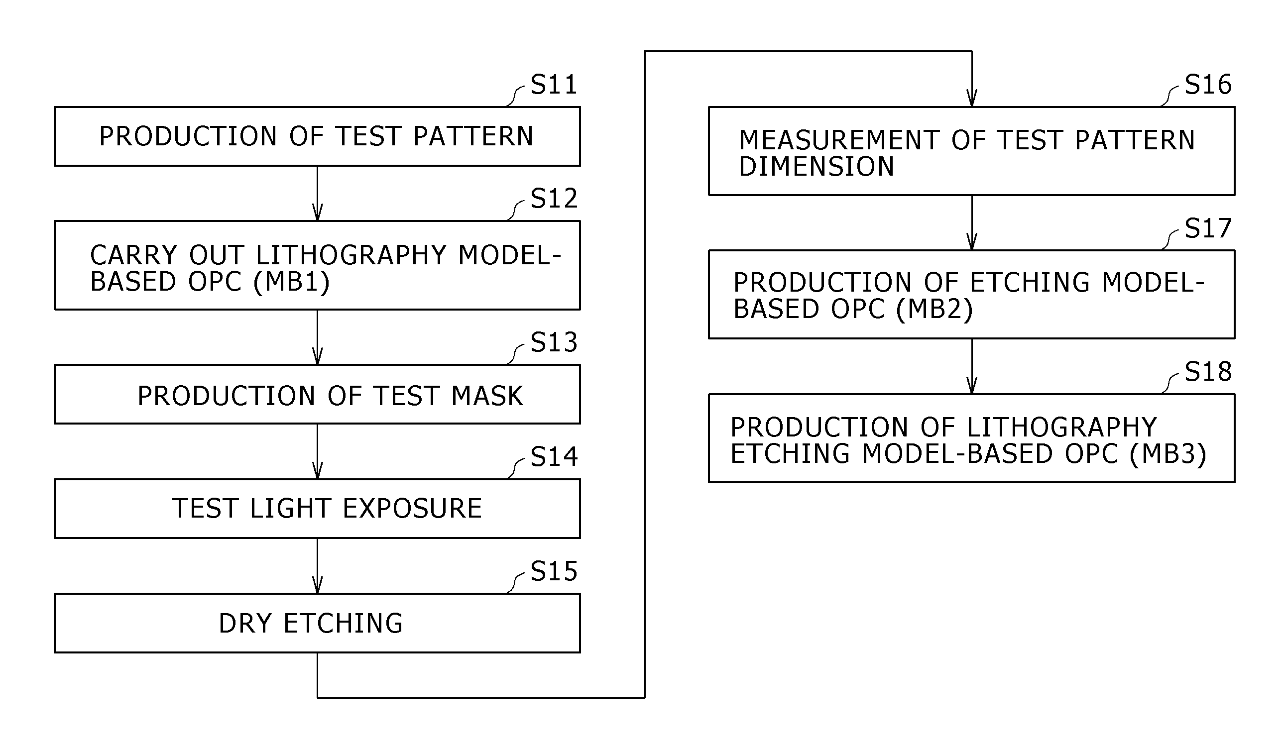
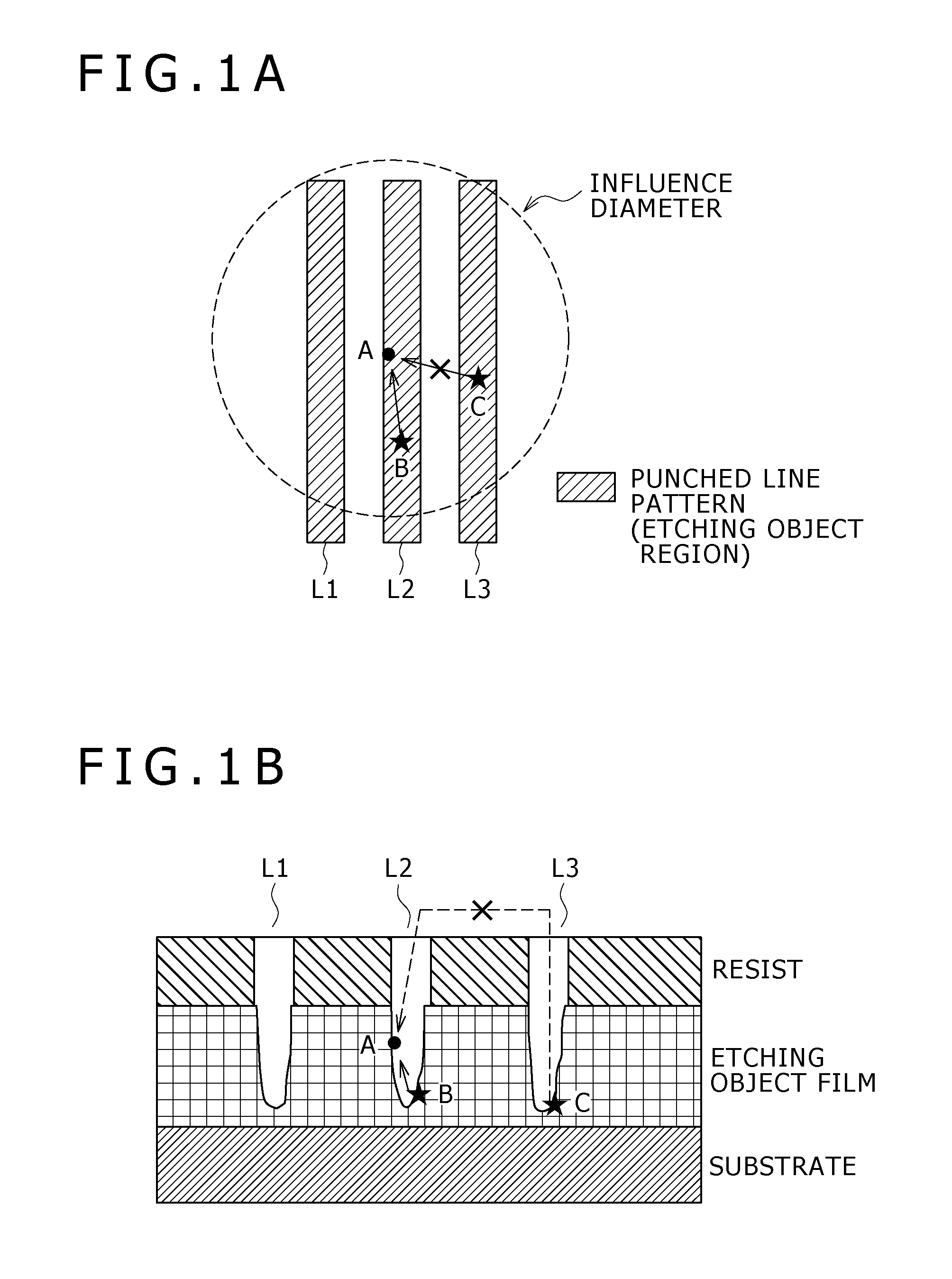
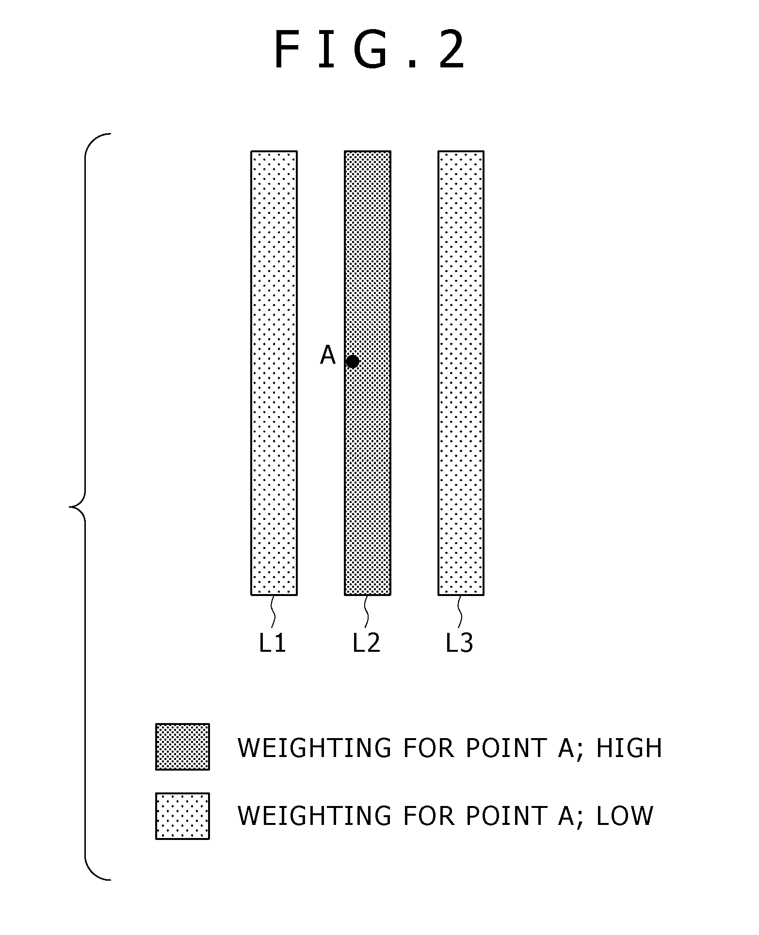
[0047]Now, a pattern correction apparatus, a pattern correction program, a pattern correction method and a fabrication method for a semiconductor device wherein the model-based OPC described above is carried out are described in connection with particular examples. Here, correction of an etching work conversion difference which may possibly occur in a metal layer working process at a drying etching step which is one of steps of a semiconductor device fabrication process is described.

[0048]FIG. 5 is a block diagram showing an example of a general configuration of a pattern correction apparatus to which the present invention is applied. Referring to FIG. 5, the pattern correction apparatus includes an information processing section 1, an information inputting section 2, an information outputting section 3, and an information storage section 4. The information processing section 1 has functions as a computer which is implemented by a combination of a CPU (Central Proce...


PUM


Abstract

A pattern correction apparatus for performing both of optical proximity effect correction and process proximity effect correction with regard to a design pattern includes: a correction calculation means configured to perform correction calculation by two-dimensional model-based optical proximity effect correction for each of sampling points set on pattern edges which form the design pattern; the correction calculation means performing the correction calculation which involves weighting with a two-dimensional distribution of the pattern edges around the sampling point taken into consideration; the weighting being performed such that a high weight is applied to a region in which reaction products which can have an influence on the sampling point are produced but a low weight is applied to any other region.

Description

CROSS REFERENCES TO RELATED APPLICATIONS[0001]The present invention contains subject matter related to Japanese Patent Application JP 2006-040414 filed with the Japanese Patent Office on Feb. 17, 2005, the entire contents of which being incorporated herein by reference.BACKGROUND OF THE INVENTION[0002]1. Field of the Invention[0003]This invention relates to a pattern correction apparatus, a pattern correction program, a pattern correction method and a fabrication method for a semiconductor device which are utilized in a fabrication process of a semiconductor device.[0004]2. Description of the Related Art[0005]In recent years, as a result of progress of the generation of the basic size of semiconductor devices to that later than the 65-nm generation, the magnitude of the dispersion of the pattern size, the distortion of the shape and so forth which are caused by an influence of proximity effects cannot be ignored any more. Such proximity effects include not only an optical proximity ...

Claims


Application Information

Patent Timeline
IPC IPC(8): G06F17/50G03F1/36G03F1/68G03F1/70H01L21/027H01L21/3065H01L21/82H01L21/822H01L27/04
CPCG03F1/36G03F1/144G03F1/68
Inventor SATO, SHUNICHIRO
Owner SONY CORP
Why Eureka
Try Eureka