Modular board device, high frequency module, and method of manufacturing the same

a module board and high frequency module technology, applied in the direction of high frequency circuit adaptation, conductive pattern formation, printed circuit non-printed electric components association, etc., can solve the problems of high cost of communication terminal equipment, large burden on the communication infrastructure side, and difficulty in forming communication terminal equipmen

Inactive Publication Date: 2008-07-31
SONY CORP
View PDF3 Cites 47 Cited by
  • Summary
  • Abstract
  • Description
  • Claims
  • Application Information

AI Technical Summary

Benefits of technology

[0019]An object of the present invention is to provide a novel module board device and a method of manufacturing the same, which can solve problems that conventional wireless communication modules have.
[0020]Another object of the present invention is to provide a module board device and a method of manufacturing the same, which does not require package structure of elements to realize improvement in reliability along with miniaturization and low cost.
[0021]A further object of the present invention is to provide a high frequency module having multi-band compliance function, which comprises MEMS switches which permit compatibility at different frequency bands and / or elements of which characteristics are deteriorated by resin sealing, and which realizes improvement in the characteristics and reliability of these elements and realizes miniaturization and low cost, and a method of manufacturing such a high frequency module.

Problems solved by technology

Such wireless network systems not only lead to enlargement and / or high cost of communication terminal equipments, but also result in large burden also with respect to the communication infrastructure side.
For this reason, it is extremely difficult to constitute the communication terminal equipments so that they are adapted to the specification of such wireless network system.
However, even such SDR technology has vast calculation quantity for signal processing.
As a result, even if compliance of burden at the communication infrastructure side can be realized, compliance of power consumption at the communication terminal equipment side and / or compliance of enlargement by integration are great problems.
Particularly, it is difficult that portable communication terminal equipments are put to practical use.
In the above-described conventional wireless communication module 100, there is the problem that the characteristic is lowered by the influence on the high frequency circuit unit resulting from reflection or loss from parasitic component of the MEMS switch 130.
There is the problem that in the case where these elements are coated by insulating resin, their characteristics are remarkably deteriorated.

Method used


Image

  • Modular board device, high frequency module, and method of manufacturing the same
  • Modular board device, high frequency module, and method of manufacturing the same
  • Modular board device, high frequency module, and method of manufacturing the same

Examples


Embodiment Construction

[0058]Embodiments of the present invention will now be described in detail with reference to the attached drawings.

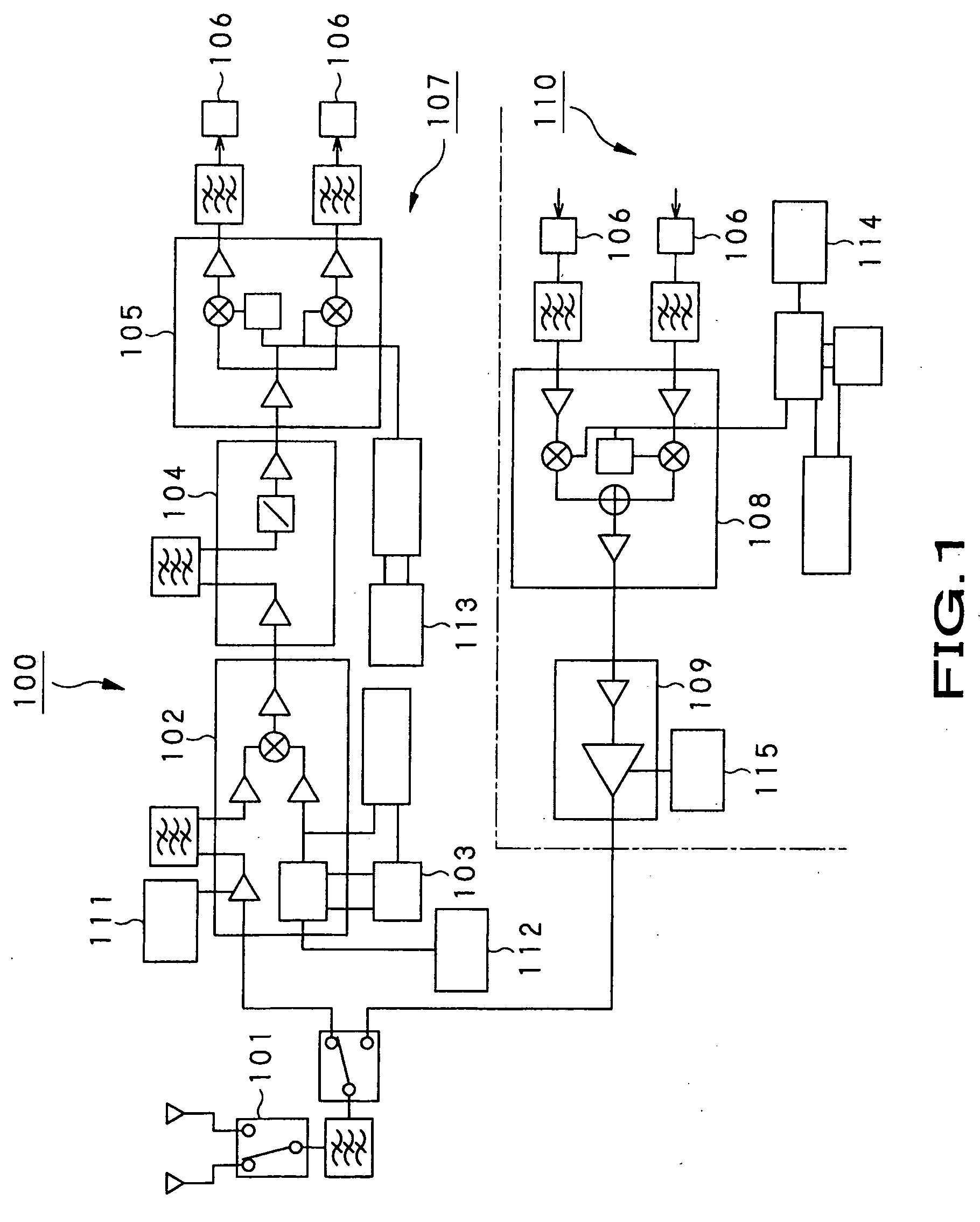
[0059]First, a high frequency module to which the present invention has been applied will be explained. The high frequency module is used in various electronic equipments having wireless communication function, e.g., personal computers, audio equipments, various mobile equipments and / or mobile telephones, etc. and constitutes analog front end of the wireless transmitting / receiving unit.

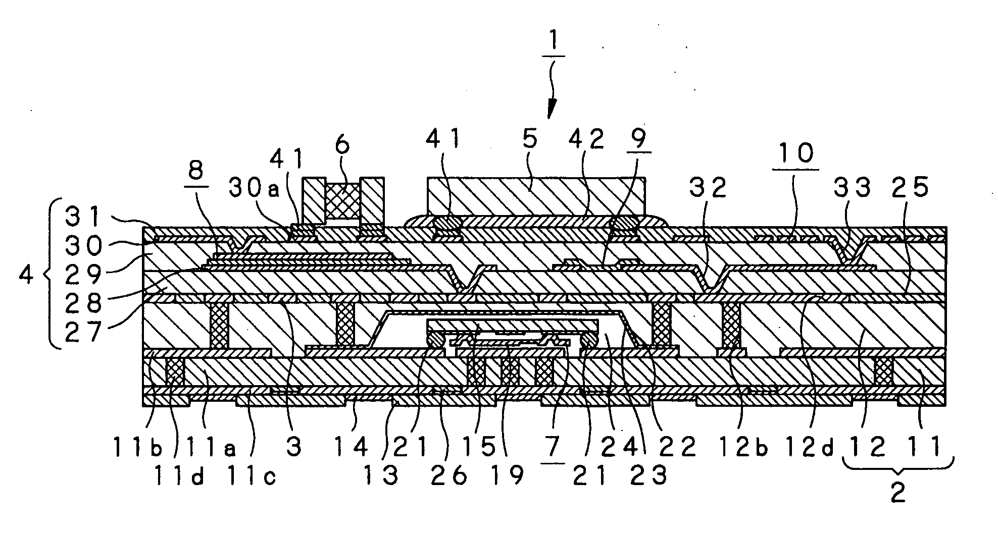
[0060]As shown in FIG. 4, the high frequency module 1 according to the present invention is caused to be of the so-called multi-band configuration in which the base band portion is shared with respect to the same modulation / demodulation system or the different modulation / demodulation systems, and transmission / reception of wireless signals of different frequency bands can be made. Although the detail will be described later, the high frequency module 1 is composed of a base substrate porti...


PUM

PropertyMeasurementUnit
thicknessaaaaaaaaaa
thicknessaaaaaaaaaa
temperatureaaaaaaaaaa

Abstract

The present invention is directed to a high frequency module used for wireless communication module, and comprises a first organic substrate (11) in which conductive pattern or patterns are formed on the principal surface thereof and one element body (7) or more are mounted, and a second organic substrate (12) in which a recessed portion (22) is formed in correspondence with the area where the element body or bodies (7) are mounted at the connecting surface to the first organic substrate (11). In the state where the second organic substrate (12) is connected to the first organic substrate (11), an element body accommodating portion (24) which seals the element body or bodies (7) is constituted by the recessed portion (22), wherein the element body accommodating portion (24) is adapted so that moisture resistance characteristic and oxidation resistance characteristic are maintained.

Description

[0001]The subject matter of application Ser. No. 10 / 519,765 is incorporated herein by reference. The present application is a divisional of U.S. application Ser. No. 10 / 519,765, filed Dec. 28, 2004, which is a 371 National Stage of PCT patent application No. PCT / JP03 / 07827, filed Jun. 19, 2003, which claims priority to Japanese Patent Application No. JP 2002-195022, filed Jul. 3, 2002. The present application claims priority to these previously filed applications.TECHNICAL FIELD[0002]The present invention relates to a module board device and a high frequency module suitable when used in wireless communication modules which are provided at various electronic equipments having wireless communication function such as personal computers, audio equipments, various mobile equipments and / or mobile telephones and permit compatibility at different frequency bands, and a method of manufacturing these module units.BACKGROUND ART[0003]Various information, e.g., music, speech and / or image, etc. ...

Claims


Application Information

Patent Timeline
Patent Type & Authority Applications(United States)
IPC IPC(8): H05K3/36H05K3/10H01L21/60H01L23/12H01L21/607H01L23/00H01L23/04H01L23/10H01L23/538H01L23/552H01L23/66H01L25/00H01L25/16H01P1/12H05K1/02H05K1/18H05K3/46
CPCH01L23/04Y10T29/49126H01L23/552H01L23/564H01L24/81H01L25/162H01L25/165H01L2224/13144H01L2224/16H01L2224/48247H01L2224/73204H01L2224/81801H01L2224/83102H01L2224/92125H01L2924/01004H01L2924/01013H01L2924/01029H01L2924/01033H01L2924/01073H01L2924/01078H01L2924/01079H01L2924/01082H01L2924/09701H01L2924/14H01L2924/15151H01L2924/16152H01L2924/1617H01L2924/16235H01L2924/19041H01L2924/19042H01L2924/19043H01L2924/19105H01L2924/30105H01L2924/3025H05K1/0218H05K1/0237H05K1/0272H05K1/16H05K1/186H05K3/4602H05K3/4614H05K3/4697H05K2201/0179H05K2201/09072H05K2201/09981H05K2201/10053H05K2203/061H05K2203/086H05K2203/1147H05K2203/1178H01L24/48H01L2924/01005H01L2924/01006H01L2924/01023H01L2924/01024H01L2924/01047H01L2924/014B81C1/0023H01L2924/1461H01L23/10Y10T29/49155H01L2924/00H01L2924/12042H01L2924/181H01L2924/00014H01L2223/6677H01L2924/00012H01L2224/45099H01L2224/45015H01L2924/207H01L23/12H01L25/00H01P1/12
Inventor OKUBORA, AKIHIKO
Owner SONY CORP
Why Eureka
Try Eureka