
Substrate processing apparatus

a processing apparatus and substrate technology, applied in the direction of coatings, chemical vapor deposition coatings, metallic material coating processes, etc., can solve the problems of high cost of silylation gas used as a process gas, conduction failure, and possible failure of wafer transporting to the vacuum process in the air, so as to reduce the capacity of the internal chamber

Active Publication Date: 2008-07-31
TOKYO ELECTRON LTD
View PDF47 Cites 16 Cited by
  • Summary
  • Abstract
  • Description
  • Claims
  • Application Information

AI Technical Summary

Benefits of technology

[0010]The present invention provides a substrate processing apparatus capable of reducing the capacity of the space in the internal chamber.
[0012]According to the present invention, when the substrate is transferred in and out by the transfer arm used to transfer the substrate, the movable component defining the space in the internal chamber exits out of the motion range of the transfer arm. Accordingly, there is no contact between the transfer arm and movable component and no need to secure a clearance for the arm and movable component in the internal chamber. As a result, the capacity of the space in the internal chamber can be reduced.
[0014]According to the present invention, when the substrate is transferred in and out by the transfer arm, the lid-like member as the movable component moves away from the mounting stage as the at least one another component. Since the moving mechanism of the lid-like member merely needs a relatively simple structure, the substrate processing apparatus can be structurally simple.
[0016]According to the present invention, when the substrate is transferred in and out by the transfer arm, the mounting stage as the movable component moves away from the lid-like member as the at least one another component. Reaction products may sometimes adhere to the lid-like member; however the lid-like member is immovable and the reaction products are thus not peeled off, unlike in the case where a movable lid-like member drops reaction products peeled off due to impact of the movement of the movable lid-like member, and therefore the immovable lid-like member can prevent foreign matter from adhering to the substrate mounted on the mounting stage.
[0018]According to the present invention, the movable component and the at least one another component each include a heating unit. The restoration process for the low dielectric constant insulating film in the substrate is enhanced by heat. Therefore, the low dielectric constant insulating film can be promptly restored.
[0020]According to the present invention, the open / close valve of the gas supply pipe in communication with the space in the internal chamber is arranged in the proximity of the internal chamber. Closing of the open / close valve reduces the capacity of a part of the gas supply pipe in communication with the internal chamber, thereby reliably reducing the usage of the process gas.

Problems solved by technology

After these vacuum processes, carrying the wafers subjected to the vacuum processes in the air can possibly produce various failures.
Specifically, natural oxidation occurs on a metal layer formed through the CVD process to form an oxide film that causes conduction failures in a semiconductor device.
However, the silylation gas used as a process gas is costly, and therefore a reduction in usage of the silylation gas is required.
Accordingly, there should be a clearance between the arm and components in the internal chamber to keep the arm from contact with the components, and consequently, the capacity of the space in the internal chamber cannot be reduced.

Method used


Image

  • Substrate processing apparatus
  • Substrate processing apparatus
  • Substrate processing apparatus

Examples


first embodiment

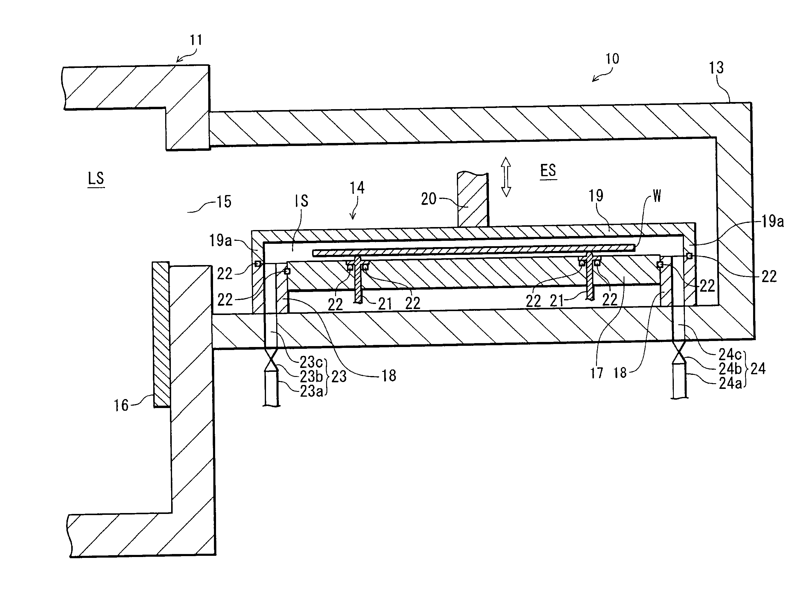
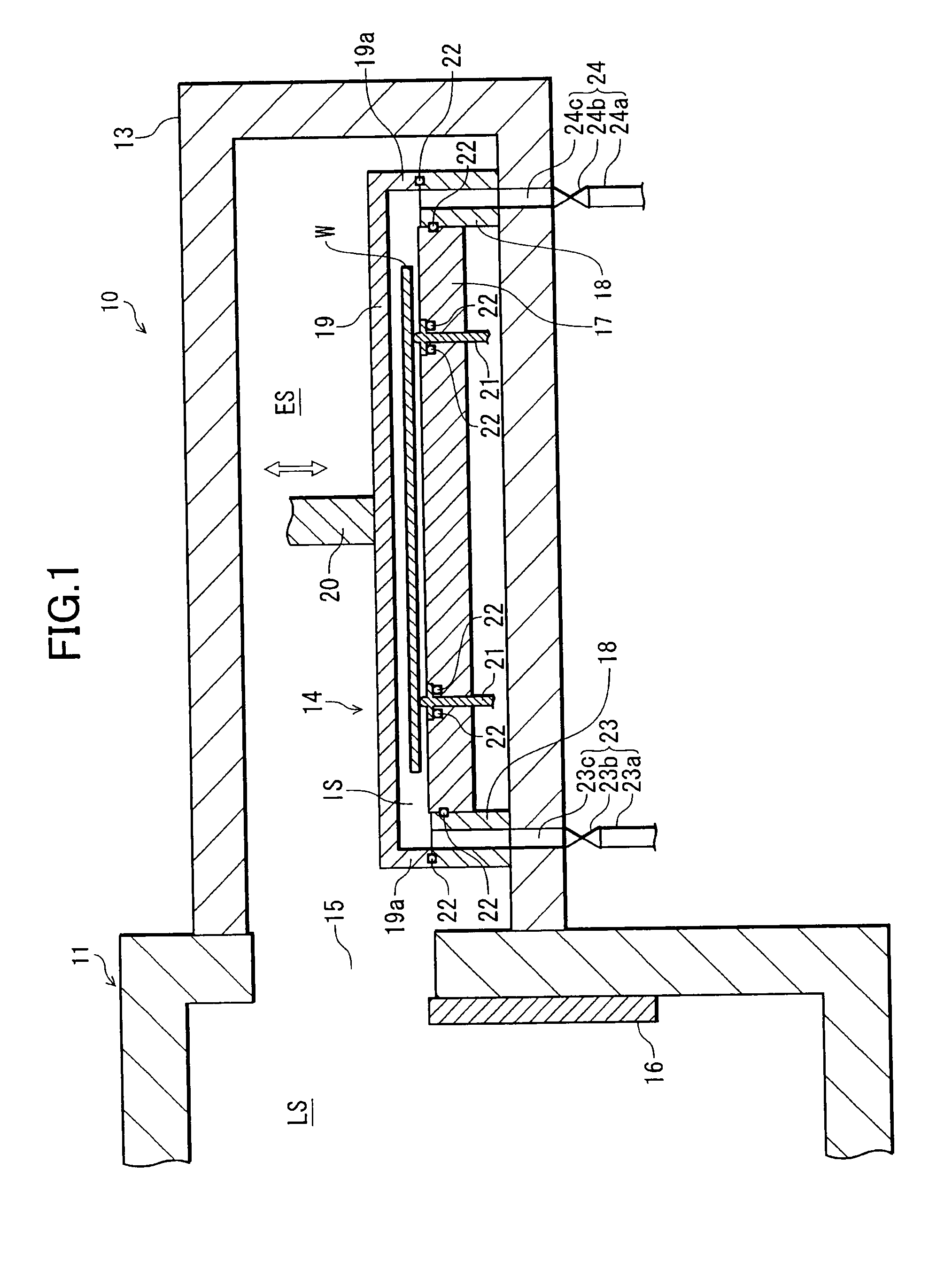
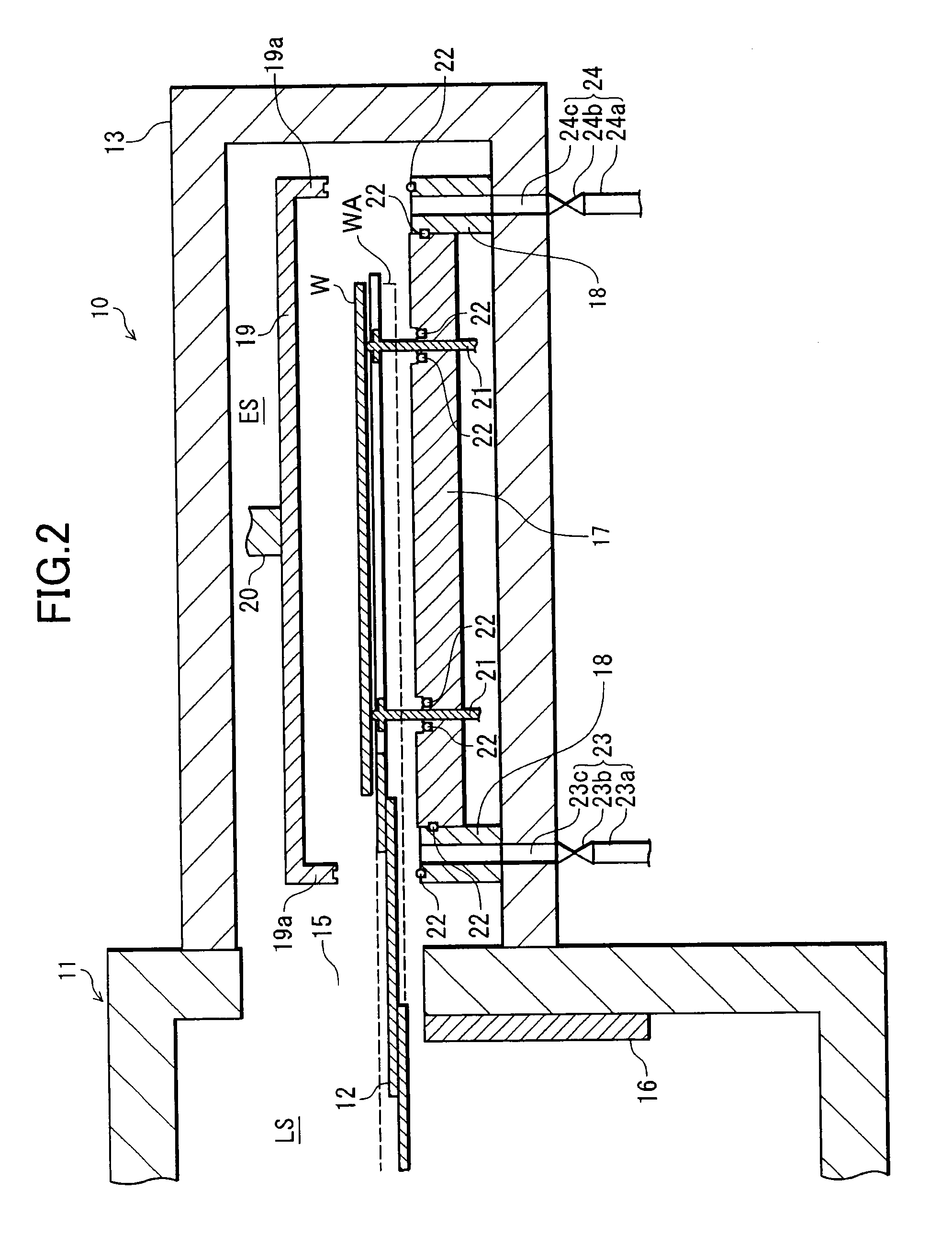
[0027]First, a description will be given of a substrate processing apparatus according to the present invention.

[0028]FIG. 1 is a cross-sectional view schematically showing the construction of the substrate processing apparatus according to the present embodiment.

[0029]In FIG. 1, the substrate processing apparatus 10 is disposed adjacent to a load lock chamber 11 as a transfer chamber used for transferring a semiconductor wafer (hereinafter simply referred to as “wafer”) W. This load lock chamber 11 has a transfer arm 12, described later, on which the wafer W is mounted to transfer it, and a space LS therein maintained under vacuum.

[0030]The substrate processing apparatus 10 is comprised of a case-like external chamber 13 connected to the load lock chamber 11 and an internal chamber 14 housed in a space ES in the external chamber 13. The space ES in the external chamber 13 is depressurized by an exhaust device (not shown) to be maintained close to a vacuum. In addition, the external...

second embodiment

[0051]Next, a description will be given of a substrate processing apparatus according to the present invention.

[0052]FIG. 3 is a cross-sectional view schematically showing the construction of the substrate processing apparatus according to the present embodiment.

[0053]In FIG. 3, the substrate processing apparatus 30 is also disposed adjacent to the load lock chamber 11.

[0054]The substrate processing apparatus 30 is comprised of a case-like external chamber 31 connected to the load lock chamber 11 and an internal chamber 32 housed in a space ES′ in the external chamber 31. The space ES′ in the external chamber 31 is maintained close to a vacuum.

[0055]The internal chamber 32 includes a stage heater 34 (movable component), which is a disc member supported by a rod 33, containing a heater (not shown) (heating unit) and functioning as a mounting stage on which a wafer W is mounted, and an enclosure 35 (at least one another component) that is a circular lid-like member and arranged so as ...


PUM

PropertyMeasurementUnit
pressureaaaaaaaaaa
distanceaaaaaaaaaa
pressureaaaaaaaaaa

Abstract

A substarate processing apparatus capable of reducing the capacity of a space in an internal chamber. The internal chamber is housed in a space in an external chamber. A gas supply unit supplies a process gas into the space in the internal chamber. The space in the external chamber is under a reduced pressure or filled with an inert gas. An enclosure being movable and included in the internal chamber defines the space in the internal chamber with a stage heater included in the internal chamber. When a wafer is transferred in and out by a transfer arm used to transfer the wafer, the enclosure exits out of a motion range within which the transfer arm can move.

Description

BACKGROUND OF THE INVENTION[0001]1. Field of the Invention[0002]The present invention relates to substrate processing apparatuses, and in particular to a substrate processing apparatus having a dual-chamber structure including an external chamber and an internal chamber housed in the external chamber.[0003]2. Description of the Related Art[0004]In semiconductor manufacturing processes for manufacturing a semiconductor device from a wafer as a substrate, a process involving chemical reactions induced by process gases tends to be widely used. The process involving chemical reactions (hereinafter referred to as “chemical reaction process”) corresponds to, for example, a process of restoring insulating films with a low dielectric constant (Low-k film) that are damaged during ashing to remove resist films by silylation gases.[0005]In addition, vacuum processes, such as an etching process, an ashing process and a CVD process, have been frequently used in the conventional semiconductor man...

Claims


Application Information

Patent Timeline
Patent Type & Authority Applications(United States)
IPC IPC(8): H01L21/306C23C16/00
CPCC23C16/401C23C16/4401H01L21/67748H01L21/6719H01L21/3105H01L21/02
Inventor TAHARA, SHIGERUTAKAYAMA, SEIICHITAKANASHI, MORIHIRO
Owner TOKYO ELECTRON LTD
Learn More