Semiconductor device
- Summary
- Abstract
- Description
- Claims
- Application Information
AI Technical Summary
Benefits of technology
Problems solved by technology
Method used
Image
Examples
embodiment 1
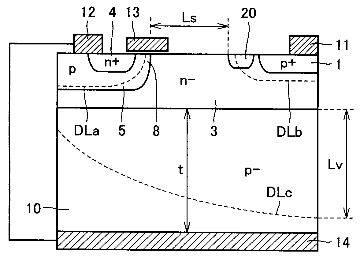
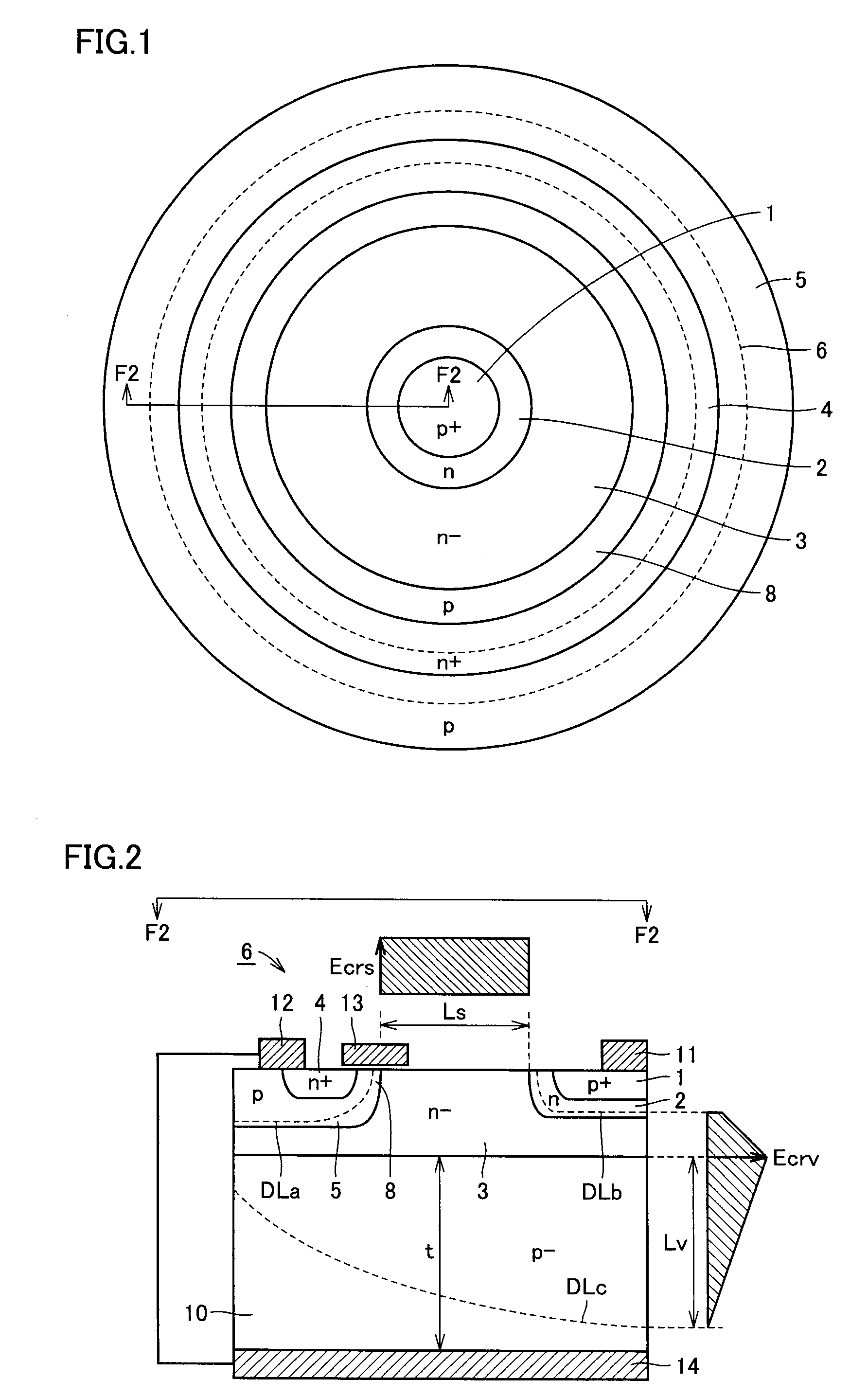
[0058]FIG. 1 schematically shows a planar layout of a semiconductor device according to embodiment 1 of the present invention. In FIG. 1, the arrangement of impurity regions is shown, and no electrode is shown for the sake of simplification of the drawing.
[0059]In FIG. 1, there is provided a p type (first conductivity type) collector layer (first semiconductor region) 1 formed at the center, and an n type (second conductivity type) buffer layer (third semiconductor region) 2 formed encompassing collector layer 1. In FIG. 1, n type buffer layer 2 is formed in a ring form so as to surround p type collector layer 1 in the planar layout.
[0060]Outside n type buffer layer 2, a low-concentration n type drift layer (fifth semiconductor region) 3 is formed in contact with n type buffer layer 2. In this planar layout, n type drift layer 3 is shown being formed in a ring form, but it is formed over the entire area in the semiconductor device.
[0061]Outside n type drift layer 3, a p type base la...
modification 2
[Modification 2]
[0097]FIG. 6 schematically shows the configuration of modification 2 of embodiment 1 of the present invention. The semiconductor device shown in FIG. 6 is different in structure from the semiconductor device shown in FIG. 2 in the following point. Specifically, through deep diffusion of an n type impurity into p type semiconductor substrate 10, an n type diffusion layer (fifth semiconductor region) is formed on the surface of p type semiconductor substrate 10. N type diffusion layer 22 is formed to a depth deeper than the depth of n type buffer layer 2 and surrounding buffer layer 2. N type diffusion layer 22 is formed such that one end thereof extends to a portion of p type base layer 5 just below n type emitter layer 4. It is ensured that the hole current passed into n type diffusion layer 22 is reliably injected into p type base layer 5 from p type collector layer 1. A part of a first main surface of p type semiconductor substrate 10 contacts the bottom of the p t...
embodiment 2
[0102]FIG. 7 schematically shows a sectional structure of the semiconductor device according to embodiment 2 of the present invention. The semiconductor device shown in FIG. 7 is different in structure from the semiconductor device shown in FIG. 2 in the following point. Specifically, a high-concentration p type semiconductor substrate (second semiconductor substrate) 30 is provided between p type semiconductor substrate 1 and rear-side electrode 14. The other configuration of the semiconductor device shown in FIG. 7 is same as the configuration of the semiconductor device shown in shown in FIG. 2, corresponding parts are allotted the same reference numerals, and detailed descriptions thereof will not be repeated.
[0103]In the semiconductor device shown in FIG. 7, the thickness ta of p type semiconductor substrate 10 is set to a value in a range of Ls or longer and 2×Ls or shorter. Ls represents a distance along the surface of drift layer 3 between p type base layer 5 and n type buff...
PUM
 Abstract
Description
Claims
Application Information


