Circuit structure and process thereof

a technology of circuit structure and process, applied in the field of circuit structure, can solve the problems of high aspect ratio of conductive via fabrication, and achieve the effects of enhancing the tolerance of alignment, increasing the circuit density of the circuit structure or fitness, and enhancing the aspect ratio

Inactive Publication Date: 2008-07-31
UNIMICRON TECH CORP
View PDF4 Cites 11 Cited by
  • Summary
  • Abstract
  • Description
  • Claims
  • Application Information

AI Technical Summary

Benefits of technology

[0020]Accordingly, the present invention fabricates a single conductive channel for electrically connecting two circuit patterns in different layers through a two-stage process. Hence, the conductive vias of a circuit structure may have a higher aspect ratio, thereby increasing the circuit density of the circuit structure or fitness to the design of special circuit structures. In addition, the outer diameter of the independent via pad may be greater than the outer diameter of the via pad above or below the independent via pad so as to enhance the tolerance of alignment between two circuit patterns, one above and one below the independent via pad. As a result, the process yield of the circuit structure is increased and the heat dissipating capacity of the circuit structure is improved.

Problems solved by technology

However, this method of performing a single operation to form each opening is disadvantageous to fabricating a conductive via with a high aspect ratio.

Method used


Image

  • Circuit structure and process thereof
  • Circuit structure and process thereof
  • Circuit structure and process thereof

Examples


Embodiment Construction

[0026]Reference will now be made in detail to the present embodiments of the invention, examples of which are illustrated in the accompanying drawings. Wherever possible, the same reference numbers are used in the drawings and the description to refer to the same or like parts.

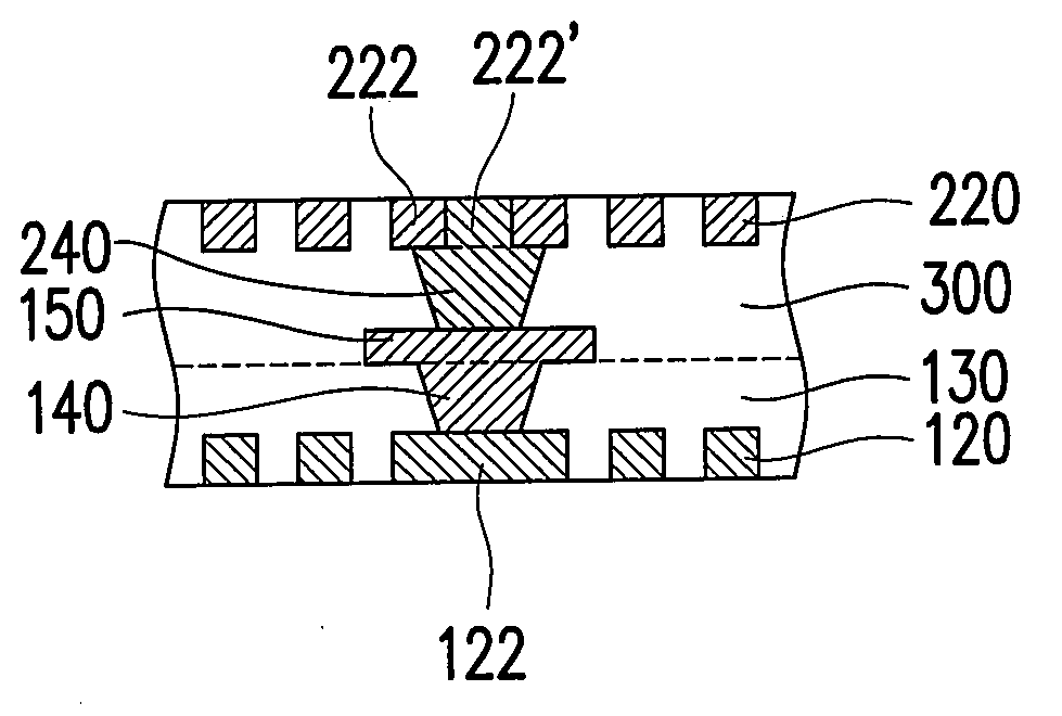
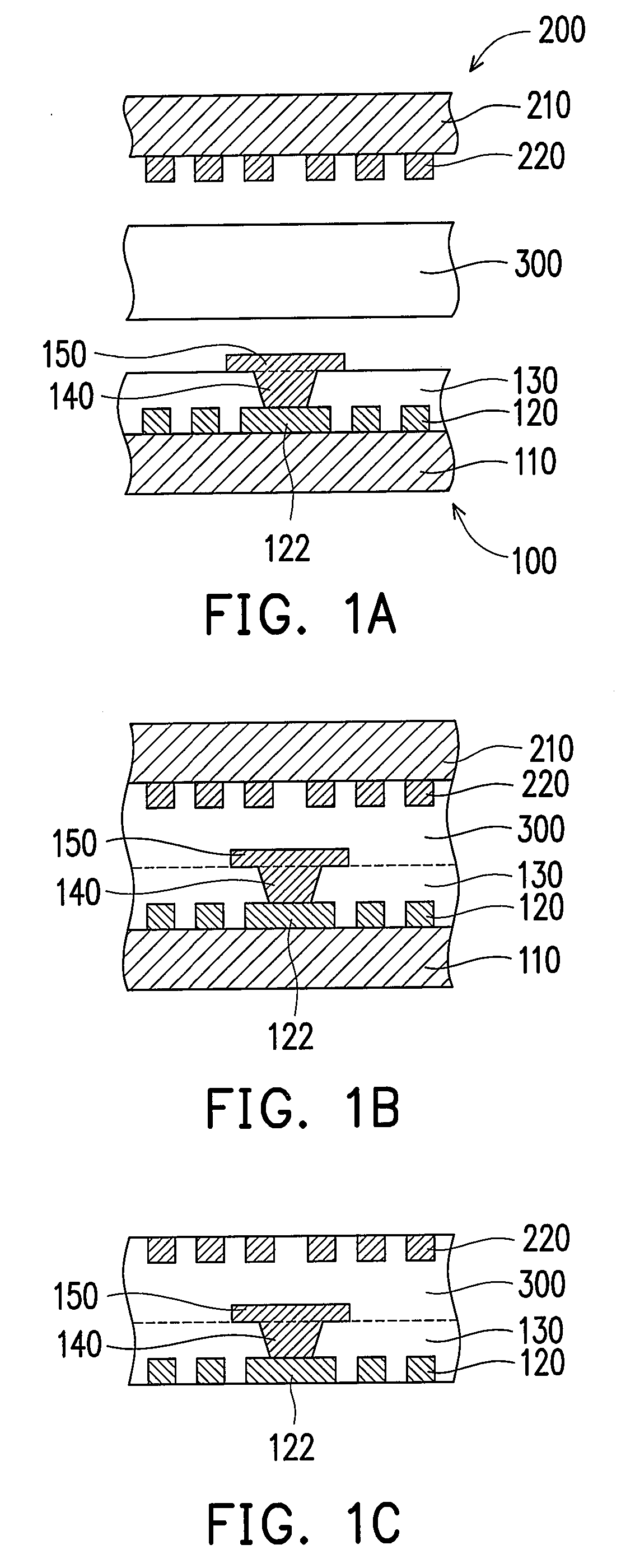
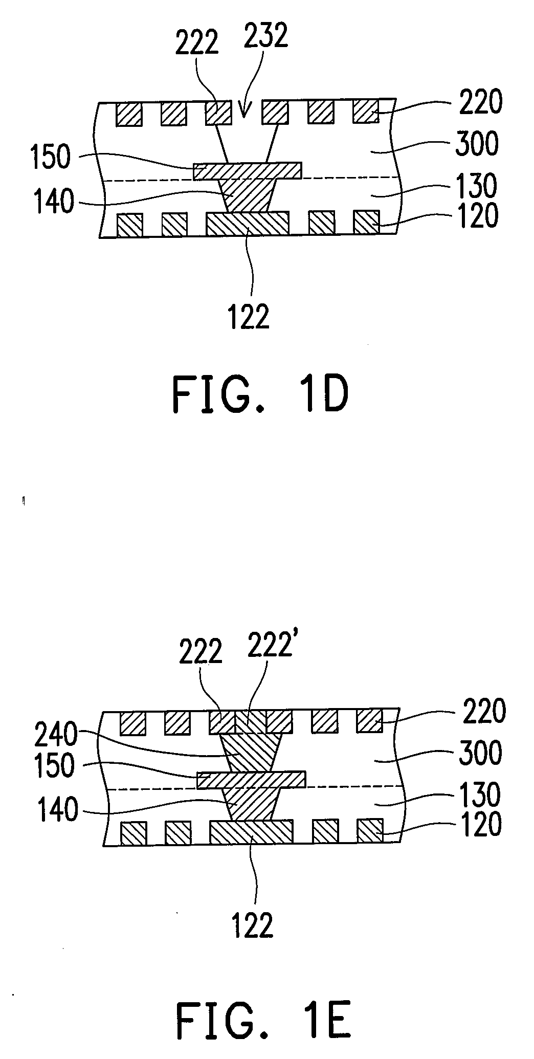
[0027]FIGS. 1A to 1E illustrate a process for fabricating a circuit structure according to an embodiment of the present invention. As shown in FIG. 1A, a first composite-layer structure 100 is provided. The first composite-layer structure 100 has a first carrier substrate 110 and a first circuit pattern 120. The first circuit pattern 120 including at least one first via pad 122 is disposed upon the first carrier substrate 110. The first composite-layer structure 100 further includes a first dielectric layer 130 covering the first carrier substrate 110 and the first circuit pattern 120. Furthermore, the first circuit pattern 120 is embedded in the first dielectric layer 130. The first composite-layer structure ...


PUM

PropertyMeasurementUnit
conductiveaaaaaaaaaa
outer diameteraaaaaaaaaa
structureaaaaaaaaaa

Abstract

A circuit structure has a first dielectric layer, a first circuit pattern embedded in the first dielectric layer and having a first via pad, a first conductive via passing through the first dielectric layer and connecting to the first via pad, and an independent via pad disposed on a surface of the first dielectric layer away from the first via pad and connecting to one end of the first conductive via. The circuit structure further has a second dielectric layer disposed over the surface of the first dielectric layer where the independent via pad is disposed, a second conductive via passing through the second dielectric layer and connecting to the independent via pad, and a second circuit pattern embedded in the second dielectric layer, located at a surface thereof away from the independent via pad, and having a second via pad connected to the second conductive via.

Description

CROSS-REFERENCE TO RELATED APPLICATION[0001]This application claims the priority benefit of Taiwan application serial no. 96102835, filed Jan. 25, 2007. All disclosure of the Taiwan application is incorporated herein by reference.BACKGROUND OF THE INVENTION[0002]1. Field of the Invention[0003]The present invention relates to a circuit structure, and more particularly to a circuit structure and process thereof.[0004]2. Description of Related Art[0005]The kinds of circuit boards normally used inside an electronic apparatus include the rigid circuit board and the flexible circuit board. The dielectric layer of a rigid circuit board is made from a strong and tough material for carrying and electrically connecting electronic components located on a single plane. The dielectric layer of a flexible circuit board is made from a flexible material for electrically connecting two electronic components located on different planes. Due to spatial limitation or other factors, the rigid circuit bo...

Claims


Application Information

Patent Timeline
Patent Type & Authority Applications(United States)
IPC IPC(8): H01L23/48
CPCH01L21/6835H01L2221/68359H05K1/116H05K3/20Y10T29/49124H05K3/4658H05K2201/09454H05K2201/09563H05K2201/096H05K3/4644
Inventor YU, CHENG-PO
Owner UNIMICRON TECH CORP
Why Eureka
Try Eureka