

Thin-film capacitor
- Summary
- Abstract
- Description
- Claims
- Application Information
AI Technical Summary
Benefits of technology
Problems solved by technology
Method used
Image

Examples
first embodiment
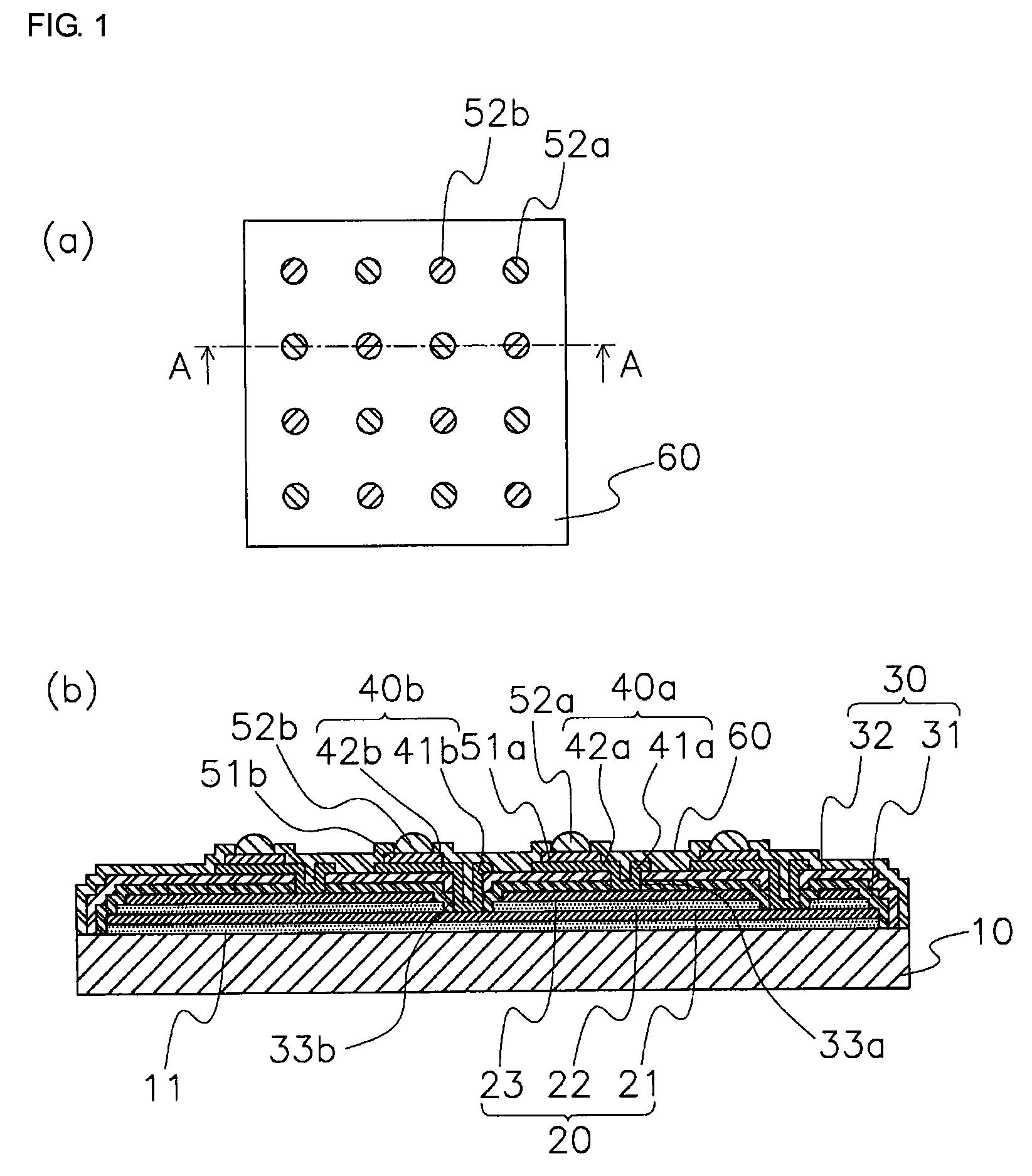
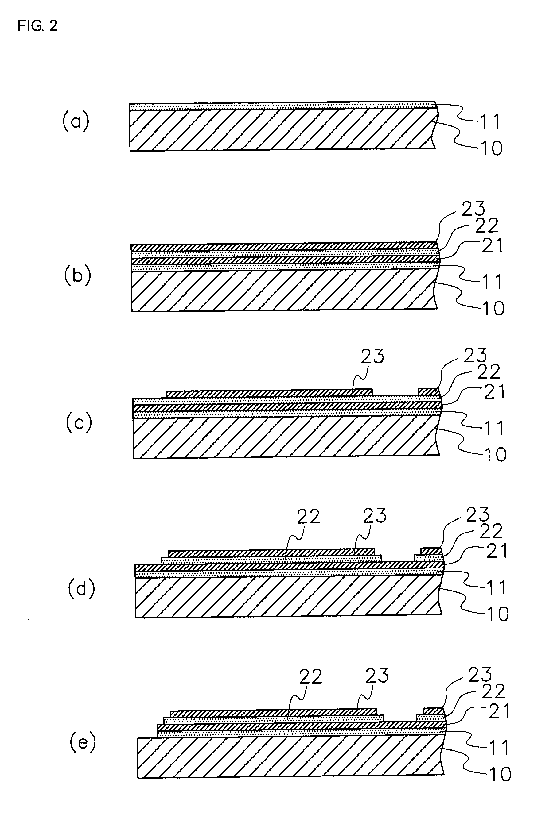
[0089]FIG. 1(a) is a plan view of a thin-film capacitor according to a first embodiment of the present invention. FIG. 1(b) is a cross-sectional view taken along line A-A of FIG. 1(a). A thin-film capacitor of the present invention includes a substrate 10 of Si, a contact layer 11 of barium strontium titanate (BST), and a capacitor unit 20 on the contact layer 11.
[0090]The capacitor unit 20 includes a lower electrode 21 and an upper electrode 23 both made of Pt, and a dielectric thin film 22 of BST. The thin-film capacitor further includes a protective layer 30 disposed over the capacitor unit 20. The protective layer 30 has a two-layer structure composed of an inorganic insulating layer 31 and a first organic insulating layer 32. The inorganic insulating layer 31 is made of silicon nitride and the first organic insulating layer 32 is made of polyimide.
[0091]The protective layer 30 has a first opening 33a, through which a first lead conductor 40a is connected to the upper electrode ...
second embodiment
[0111]A thin-film capacitor according to a second embodiment of the present invention will now be described. FIG. 4 is a plan view illustrating the thin-film capacitor of the present embodiment. FIG. 5(a) is a cross-sectional view taken along line B-B of FIG. 4. FIG. 5(b) is a cross-sectional view taken along line C-C of FIG. 4. In FIG. 4 and FIG. 5, components common or corresponding to those in FIG. 1 to FIG. 3 are given the same reference numerals, and the description thereof will be omitted.
[0112]The thin-film capacitor of the present embodiment is characterized in that some first wiring parts 42a each are connected to two first connecting parts 41a, and some second wiring parts 42b each are connected to two second connecting parts 41b. Therefore, two connecting parts 41a can be provided for one bump 52a and two connecting parts 41b can be provided for one bump 52b.
[0113]Generally, as the number of connecting parts 41a and 41b increases, the ESL of the thin-film capacitor decre...
third embodiment
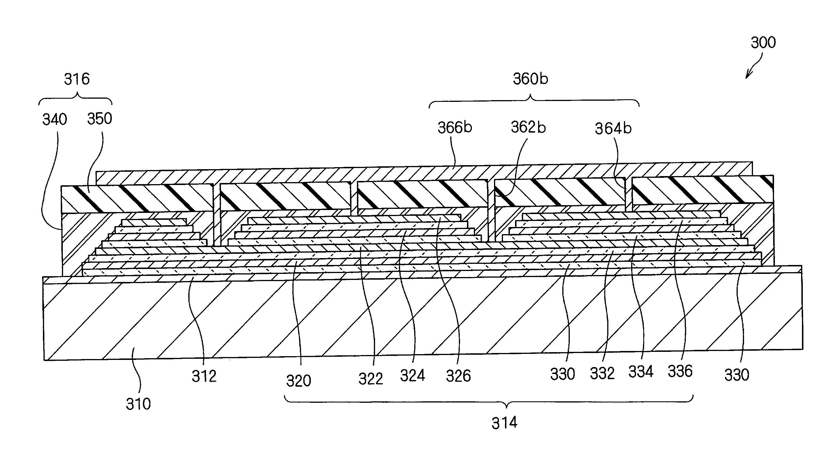
[0119]FIG. 8 illustrates a thin-film capacitor according to a third embodiment of the present invention. The thin-film capacitor illustrated in FIG. 8 is a modification of that of the first embodiment. The planar arrangement of the bumps 52a and 52b is identical to that illustrated in FIG. 1 and thus is not illustrated here.
[0120]The thin-film capacitor of the third embodiment is characterized in that the upper electrode 23, the dielectric thin film 22, and the lower electrode 21 are partially removed at their portions directly below the bumps 52a and 52b. Therefore, no capacitor units are present directly below the bumps 52a and 52b. Even when the bumps 52a and 52b are stressed in the vertical or horizontal direction, it is possible to prevent damage to capacitor units directly below the bumps 52a and 52b.
[0121]The thin-film capacitor of the present embodiment can be made by a process similar to that for the first embodiment. However, before the step of depositing the inorganic in...
PUM
 Abstract
Description
Claims
Application Information