Optical Emission Spectroscopy Process Monitoring and Material Characterization

Inactive Publication Date: 2008-08-14
WAFERMASTERS
View PDF3 Cites 18 Cited by
  • Summary
  • Abstract
  • Description
  • Claims
  • Application Information

AI Technical Summary

Benefits of technology

[0008]Methods and systems of characterization and/or monitoring semiconductor material and device processing with focused laser beams are disclosed. Specifically, in accordance with an embodiment of the disclosure, a method of monitoring the processing of semiconductor substrates, materials and devices includes providing a laser beam of a selected wavelength and a selected peak power. The laser beam may be continuous (CW) to a selected average power or may be modulated to provide pulses of a discrete time pulse width. The laser beam is focused at the surface plane of the semiconductor material. The total energy in ea

Problems solved by technology

While each may have particular advantages, there are also disadvantages whereby incorporation of the method in situ is difficult or not possible.
In addition, many such processes are destructive of at least portions of the substrate, and therefore may not enable comprehensive mapping of process characteriz

Method used


Image

  • Optical Emission Spectroscopy Process Monitoring and Material Characterization
  • Optical Emission Spectroscopy Process Monitoring and Material Characterization
  • Optical Emission Spectroscopy Process Monitoring and Material Characterization

Examples


Embodiment Construction

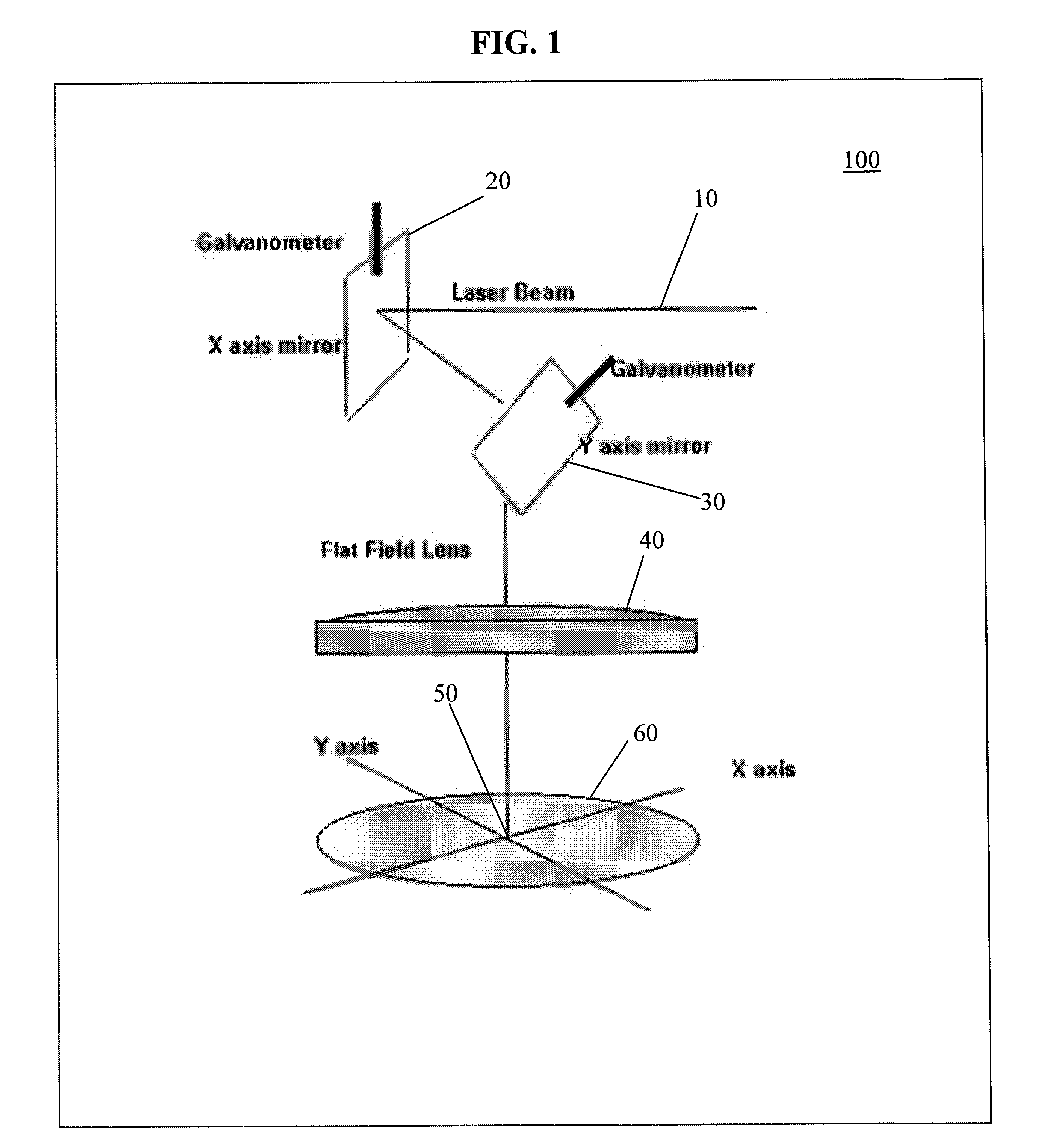
[0019]FIG. 1 is a drawing of a galvanometric beam substrate scanning system 100 for directing a focused laser beam at a semiconductor substrate during a processing step of device manufacturing. A collimated laser beam 10 is directed to a first mirror galvanometer 20 configured to scan laser beam 10, for example, in an axial direction about a first axis. Laser beam 10 is then directed toward a second mirror galvanometer 30 configured to scan laser beam 10, for example, in an axial direction about a second axis, which is perpendicular to the first axis. The effect of the two galvanometer mirrors 20 and 30 is to scan laser beam 10 in perpendicular X and Y directions in the plane of a semiconductor substrate 60. Laser beam 10 is directed by the combination of mirror galvanometers 20 and 30 through a flat field focusing lens 40. The function of flat field lens 40 is to bring laser beam 10 to a focused spot 50 at the surface of semiconductor substrate 60 with minimum distortion of the foc...


PUM

PropertyMeasurementUnit
Fractionaaaaaaaaaa
Fractionaaaaaaaaaa
Timeaaaaaaaaaa

Abstract

Methods and systems for control and monitoring processing of semiconductor materials with a focused laser beam. Laser light may be focused on a sample to excite optical emission at the sample surface during processing, which may include laser processing. Optical emission spectra produced may be analyzed for various properties effectively during the process. For example, process effects such as chemical composition analysis, species concentration, depth profiling, homogeneity characterization and mapping, purity, and reactivity may be monitored by optical spectral analysis. The wavelength may be selected to be appropriate for the process effect chosen.

Description

CROSS REFERENCE TO RELATED APPLICATIONS[0001]This application is a continuation-in-part application of U.S. patent application Ser. No. 11 / 673,306, entitled “FOCUSED LASER BEAM PROCESSING”, filed on Feb. 9, 2007.BACKGROUND[0002]1. Field of Invention[0003]This disclosure generally relates to process characterization, monitoring and control of semiconductor substrates with a focused laser beam in conjunction with laser and other processing methods.[0004]2. Related Art[0005]A number of techniques are available for chemical analysis of in situ semiconductor processes that incorporate some form of spectroscopy to assess species concentrations affecting the process. While each may have particular advantages, there are also disadvantages whereby incorporation of the method in situ is difficult or not possible. In many cases, evacuated chamber low pressure operation is required. In addition, many such processes are destructive of at least portions of the substrate, and therefore may not ena...

Claims


Application Information

Patent Timeline
IPC IPC(8): G01J3/28H01S3/10
CPCB23K26/063B23K26/0807B23K26/4075H01L21/268G01N2021/1782G01N2021/8416G01N21/718B23K26/082B23K26/0622B23K26/40B23K2103/50H01L22/00
Inventor YOO, WOO SIKKANG, KITAEK
Owner WAFERMASTERS
Why Eureka
Try Eureka