

Method of low temperature wafer bonding through Au/Ag diffusion
a low temperature wafer and diffusion technology, applied in the field of wafer bonding, can solve the problems of increasing heat stress, affecting the bonding effect of wafers, and affecting the bonding effect of devices on wafers, so as to prevent damage to devices on wafers and avoid heat stress on bonding multiple wafers
- Summary
- Abstract
- Description
- Claims
- Application Information
AI Technical Summary
Benefits of technology
Problems solved by technology
Method used
Image

Examples
Embodiment Construction
[0016]The following description of the preferred embodiment is provided to understand the features and the structures of the present invention.
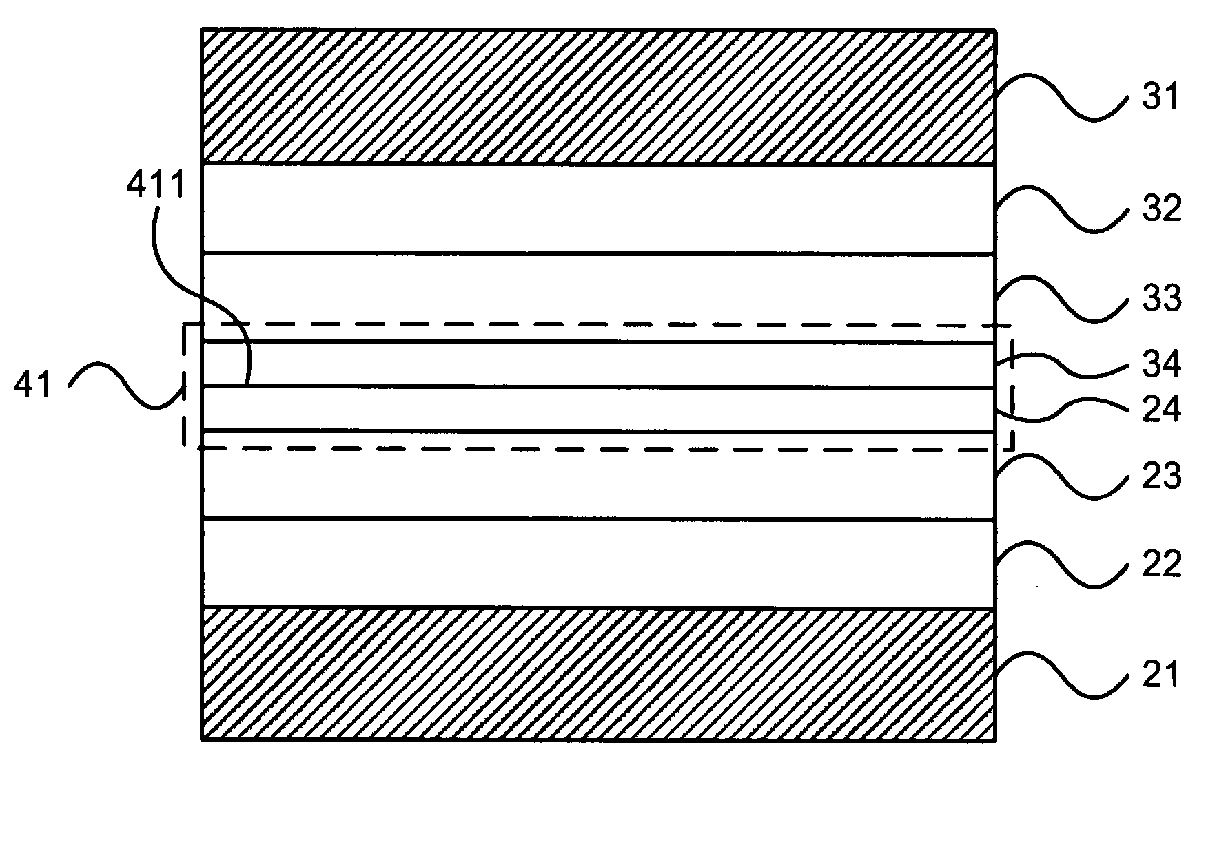
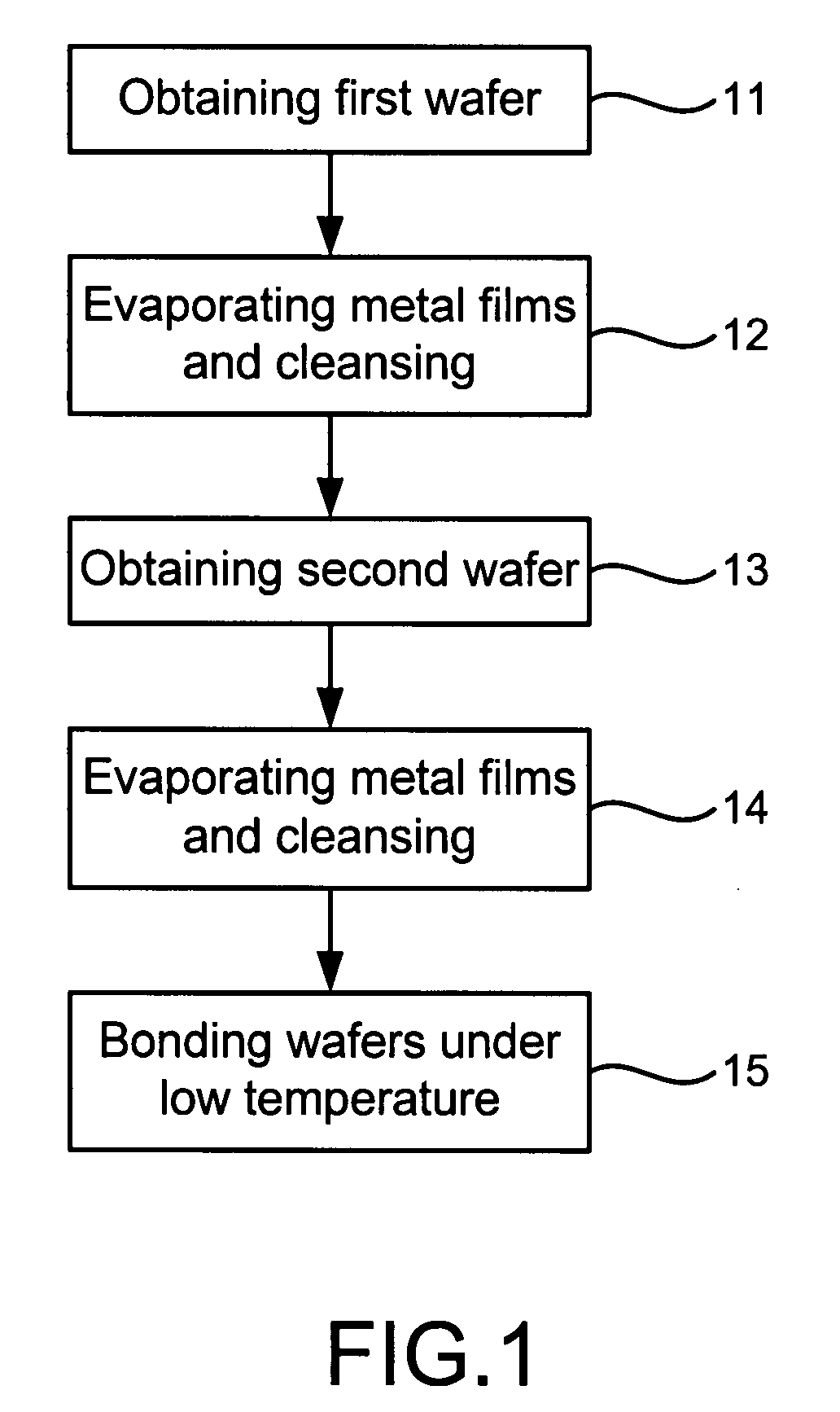
[0017]Please refer to FIG. 1 to FIG. 6, which are a flow view showing a preferred embodiment according to the present invention; structural views showing a first wafer and the first wafer coated with a Cr film, a Pt film and an Au film; structural views showing a second wafer and the second wafer coated with a Cr film, a Pt film and an Ag film; and a structural view showing the preferred embodiment. As shown in the figures, the present invention is a method of a low temperature wafer bonding through Au / Ag diffusion, comprising the following step:
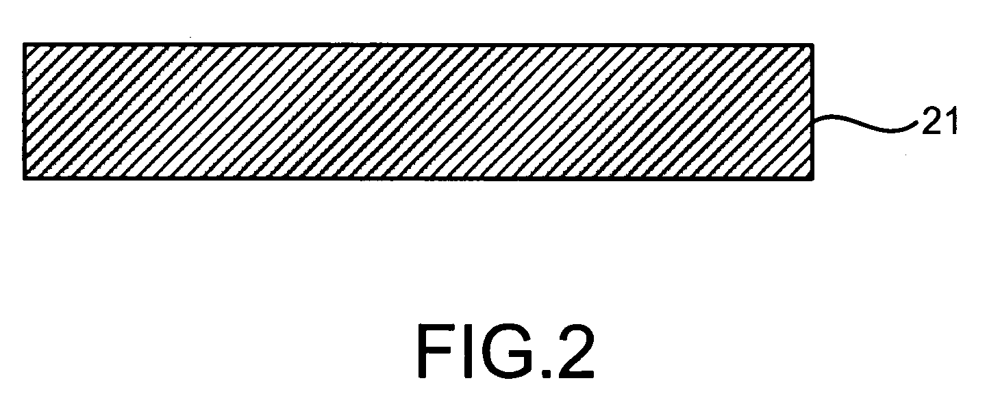
[0018](a) Obtaining a first wafer [11]: As shown in FIG. 2, a first wafer [21] is obtained, where the first wafer [21] is a silicon (Si) wafer.
[0019](b) Evaporating metal films and processing a cleansing [12]: As shown In FIG. 3, an electron-gun (E-gun) evaporator with a current between 50 and 250 mil...
PUM
| Property | Measurement | Unit |
|---|---|---|
| pressure | aaaaa | aaaaa |
| pressure | aaaaa | aaaaa |
| melting point | aaaaa | aaaaa |
Abstract
Description
Claims
Application Information