Glass corrosion mask layer method

A technology of glass and mask, applied in the field of micromachining of mechanical systems

Active Publication Date: 2017-06-30
INST OF ELECTRONICS ENG CHINA ACAD OF ENG PHYSICS
View PDF3 Cites 7 Cited by
  • Summary
  • Abstract
  • Description
  • Claims
  • Application Information

AI Technical Summary

Problems solved by technology

However, this connection technology has not been reported in the field of glass corrosion, or even in the field of glass deep hole corrosion.

Method used


Image

  • Glass corrosion mask layer method
  • Glass corrosion mask layer method
  • Glass corrosion mask layer method

Examples


Embodiment Construction

[0039] The technical scheme of the present invention will be described in detail below in conjunction with the accompanying drawings.

[0040] The material used is an N-type silicon wafer with a thickness of 300 μm, a resistivity of 1~10Ω / cm, and a crystal orientation; the glass is 7740 glass with a thickness of 500 μm.

[0041] The masking method of the present embodiment, its steps are as follows:

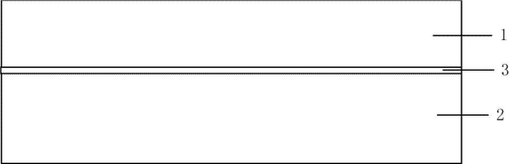
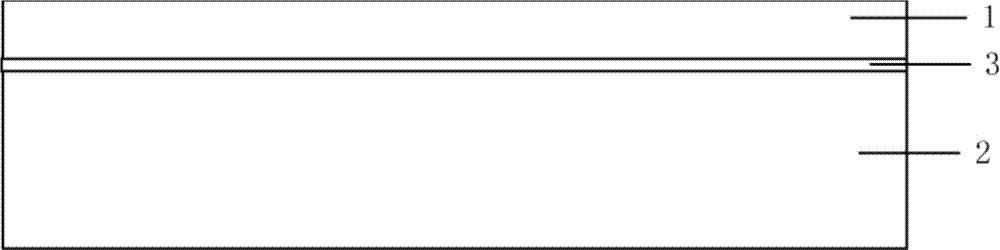
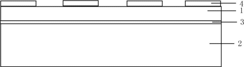
[0042] (1) if figure 1 As shown, the glass 2 and the silicon wafer 1 are bonded by the method of hydroxide catalyzed bonding, specifically:

[0043] (a) Clean the silicon wafer 1 and the glass 2 with a mixture of sulfuric acid and hydrogen peroxide;

[0044] (b) Oxidize the silicon wafer 1 in an oxidation furnace, and the thickness of the oxide layer 3 is 1 μm;

[0045] (c) Drop KOH aqueous solution on the glass 2, the ratio is 1:128, and the drop volume is 0.4 μL / cm 2 ;

[0046] (d) Gently press the silicon wafer 1 with the oxide layer 3 on the glass 2 on the side dripping...


PUM

PropertyMeasurementUnit
thicknessaaaaaaaaaa
thicknessaaaaaaaaaa
electrical resistivityaaaaaaaaaa

Abstract

The invention discloses a glass corrosion mask layer method. The method comprises the following steps: a) a silicon chip having a surface oxide layer and glass are subjected to catalysis bonding through hydroxide; b) removing oxide on the upper surface of the silicon chip; c) thinning the silicon chip; d) photoetching the surface of the silicon chip by a photoresist, forming an image required by glass corrosion; e) using DRIE (deep reactive ion etching) anisotropy etching, etching the silicon chip, wherein the etching depth is to a glass layer; f) removing the photoresist on the silicon chip; g ) corroding the glass; and h) removing silicon and silicon oxide on the glass and cleaning to obtain a required glass structure. According to the intention, glass corrosion depth is not restricted, thermal stress due to anode bonding temperature can be avoided, expensive equipment is not required, and operation is simple.

Description

technical field [0001] The invention relates to the field of mechanical system micromachining, in particular to a mask method for glass corrosion. Background technique [0002] Glass has a wide range of uses. In the past, the masks used for glass corrosion include photoresist, Cr / Au, Ti / Au, silicon carbide, etc., but using these materials as masks, the glass corrosion depth is small, generally less than 50 μm. In addition, it has been reported in the literature that using polysilicon, amorphous silicon or single crystal silicon as a mask, the glass corrosion depth is relatively large. For example, using LPCVD (Low Pressure Chemical Vapor Deposition) to deposit polysilicon as a mask, when the mask thickness is 500nm, a glass etching depth greater than 400μm can be obtained, but this method requires good control of the stress of the polysilicon film. There are difficulties; it is also reported that the method of anodic bonding uses single crystal silicon as a mask to obtain a...

Claims


Application Information

Patent Timeline
Patent Type & Authority Applications(China)
IPC IPC(8): C03C15/00
Inventor 张照云苏伟唐彬许蔚熊壮
Owner INST OF ELECTRONICS ENG CHINA ACAD OF ENG PHYSICS
Why Eureka
Try Eureka