Memory array error correction apparatus, systems, and methods

a memory array and error correction technology, applied in the field of memory devices, can solve the problems of not being able to perfectly achieve the recall of data from memory arrays in every case, penalizing the overall operation of the array, and capacitors not being ideal devices

Active Publication Date: 2008-08-14
MICRON TECH INC
View PDF5 Cites 111 Cited by
  • Summary
  • Abstract
  • Description
  • Claims
  • Application Information

AI Technical Summary

Problems solved by technology

Recalling data from memory arrays may not be perfectly accomplished in every case.
However, most error correction schemes penalize overall operation of the array, perhaps in terms of circuit real estate and / or operational speed.
However, because a capacitor is not an ideal device and is subject to leakage, the DRAM memory requires that the capacitor charge be refreshed periodically.
Over a period of time, the charge in a DRAM memory cell will leak away, and the memory content may be lost.
In other words, the data bit has changed state due to leakage, the data is lost, and at least that portion of the data stored in the memory is corrupt.
Because the refresh process consumes power each time it is performed, the more frequently the refresh process is performed, the more overall power the memory device will consume.
Thus, if the refresh operation is performed at a time interval less than the worst case bit in the memory cell, an increase in the overall power consumption of the memory device will occur, as compared to a refresh time interval that is greater than the time for the worst case memory cell to change state due to leakage.
In addition, during the time a refresh is being performed, reading from and writing to the memory (or at least to the particular block or blocks of memory being refreshed) can not be performed.
Thus, the memory (or at least the portion thereof being refreshed) is not available for read or write operations.
The refreshing of the DRAM memory represents lost time for reading from and writing to the DRAM memory, and therefore imposed an overall performance penalty on the memory device.
However, for a large number of bits included in memory, for example a one giga-byte memory, only a small fraction of the memory cells will actually have a leak rate such that a change in the state of the data stored at the memory cell occurs within the given refresh cycle interval of 64 milliseconds.
In these embodiments, the area penalty imposed by the added check bits is offset by the power savings allowed by the extension of the refresh cycle times. The extended refresh time interval reduces the number of refresh cycles performed to maintain the data in the memory and thus decreases the memory device power consumption.
Another factor that affects the overall performance of the memory device is the clock rate at which the memory device operates.
However, certain processes, including operations involving the generation of error correction codes for data to be written to the memory, and operations involving masking data to be written to the memory array, may slow down overall memory operational speed.
However, slowing the clock rate may increase the overall time required to perform read and write operations to and from the memory, and thus decrease the overall performance and speed of the memory device.
Although the design of the DRAM memory cells and memory arrays may appear simple, their actual design and implementation are highly complex.

Method used


Image

  • Memory array error correction apparatus, systems, and methods
  • Memory array error correction apparatus, systems, and methods
  • Memory array error correction apparatus, systems, and methods

Examples


Embodiment Construction

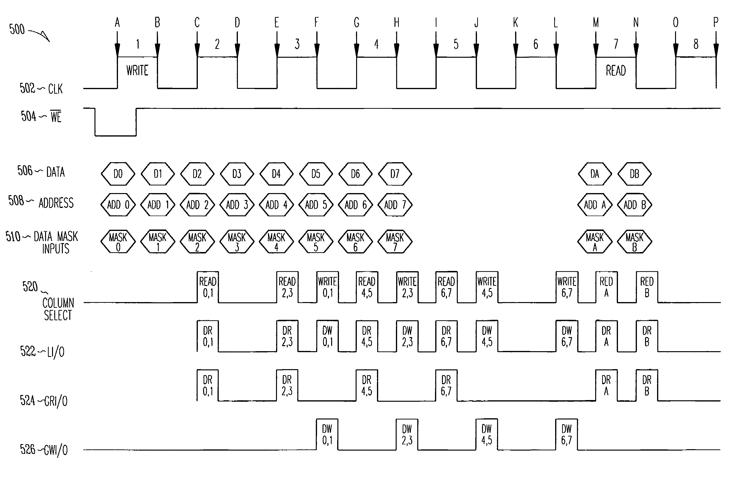
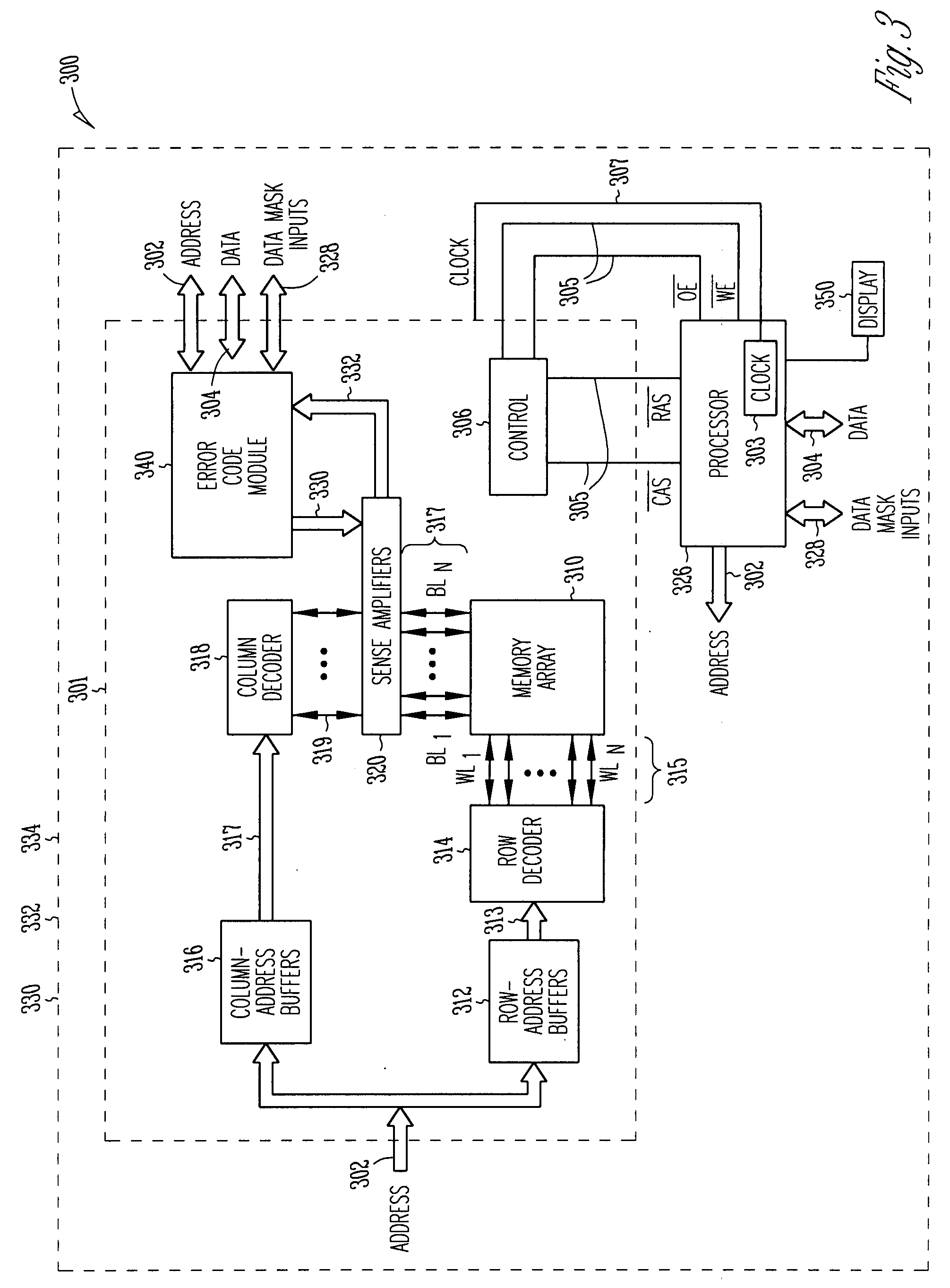
[0010]This document describes apparatus, methods, and systems that can be used to extend the processes of reading, modifying, and writing data in a memory array without interrupting a substantially continual stream of data to be received and written into the memory array. Such memory arrays may form a part of many different types of commercially available memory devices, as noted below.

[0011]As disclosed in further detail below, in various embodiments a column cycle associated with memory operations is divided in two halves. A column cycle refers to an operation, including but not limited to, a write operation associated with a particular address.

[0012]A column refers to a group of memory cells coupled to a particular word line that are selected when an address associated with the word line and an individual memory cell or a group of memory cells coupled to the word line are selected by the application of the address to the column select input of the memory array.

[0013]A column cycl...


PUM


Abstract

Various embodiments include apparatus, methods, and systems that operate to extend the processes of reading, modifying, and writing data stored in or being provided to a memory array without interrupting a continual stream of data to be written into the memory array. Embodiments may include an apparatus comprising a memory array, and an error code module coupled to the memory array with a data buffer having a plurality of data burst registers operable to receive a plurality of data bursts to be written to the memory array on a corresponding plurality of consecutive clock cycles. The error code module is operable to perform a read/modify/write process on each of the plurality of data bursts within a time period no longer than a period of two consecutive cycles of the plurality of consecutive clock cycles.

Description

TECHNICAL FIELD[0001]Various embodiments described herein relate generally to memory devices, including memory devices having error correction codes (ECC) associated with data stored in dynamic random access memory (DRAM).BACKGROUND[0002]Semiconductor memory devices are integrated circuits in which information may be stored and from which information may be recalled when desired. Each memory device is built from a plurality of memory cells in which each memory cell has the capacity to store at least one binary bit of data. Essentially, the cells are located at intersections of wordlines and bitlines (e.g., visualized as rows and columns of an array). Cells may store a single bit of data as a logical “1” or a logical “0” and may sometimes be individually accessed or addressed. Cells may sometimes be addressed using two multi-bit numbers. When this scheme is used, the first multi-bit number, or row address, may identify the row of the memory array in which the memory cell is located. ...

Claims


Application Information

Patent Timeline
Patent Type & Authority Applications(United States)
IPC IPC(8): G06F11/00G06F12/00
CPCG06F11/1056G06F11/1076G06F11/106G06F11/10G06F13/32G06F1/04
Inventor SCHRECK, JOHN F.DAUENBAUGH, TODD A.
Owner MICRON TECH INC
Why Eureka
Try Eureka