Gate pullback at ends of high-voltage vertical transistor structure

a transistor and vertical technology, applied in the field of semiconductor device structures and processes for fabricating high-voltage transistors, can solve the problems of gate oxide breakdown voltage and reliability problems, tend to produce large warping of silicon wafers,

Inactive Publication Date: 2008-08-21
POWER INTEGRATIONS INC
View PDF99 Cites 30 Cited by
  • Summary
  • Abstract
  • Description
  • Claims
  • Application Information

AI Technical Summary

Problems solved by technology

One problem that arises with this layout, however, is that it tends to produce large warping of the silicon wafer during high temperature processing steps.
Additionally, gate oxide weakness in the rounded end portions of the transistor layout can result in gate oxide breakdown voltage and reliability problems.

Method used


Image

  • Gate pullback at ends of high-voltage vertical transistor structure
  • Gate pullback at ends of high-voltage vertical transistor structure
  • Gate pullback at ends of high-voltage vertical transistor structure

Examples


Embodiment Construction

[0020]In the following description specific details are set forth, such as material types, dimensions, structural features, processing steps, etc., in order to provide a thorough understanding of the present invention. However, persons having ordinary skill in the relevant arts will appreciate that these specific details may not be needed to practice the present invention. It should also be understood that the elements in the figures are representational, and are not drawn to scale in the interest of clarity.

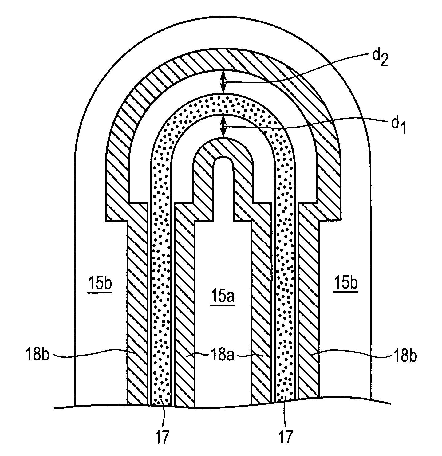
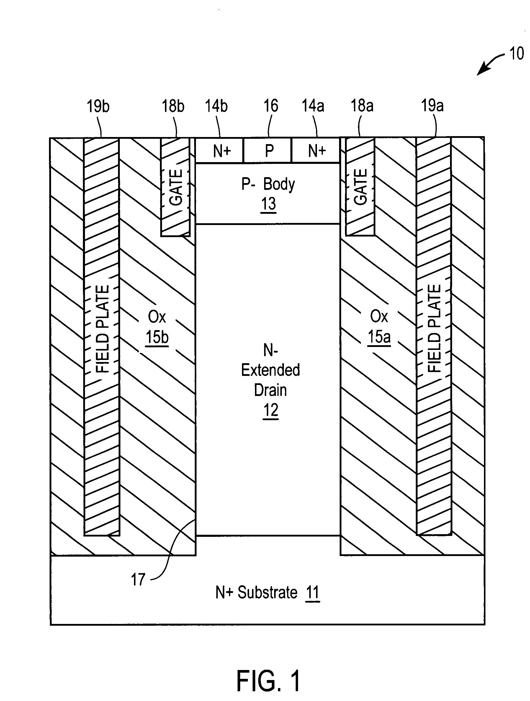
[0021]FIG. 1 illustrates an example cross-sectional side view of a vertical HVFET 10 having a structure that includes an extended drain region 12 of N-type silicon formed on an N+ doped silicon substrate 11. Substrate 11 is heavily doped to minimize its resistance to current flowing through to the drain electrode, which is located on the bottom of the substrate in the completed device. In one embodiment, extended drain region 12 is part of an epitaxial layer that extends from su...


PUM


Abstract

In one embodiment, a transistor includes a pillar of semiconductor material arranged in a racetrack-shaped layout having a substantially linear section that extends in a first lateral direction and rounded sections at each end of the substantially linear section. First and second dielectric regions are disposed on opposite sides of the pillar. First and second field plates are respectively disposed in the first and second dielectric regions. First and second gate members respectively disposed in the first and second dielectric regions are separated from the pillar by a gate oxide having a first thickness in the substantially linear section. The gate oxide being substantially thicker at the rounded sections. It is emphasized that this abstract is provided to comply with the rules requiring an abstract that will allow a searcher or other reader to quickly ascertain the subject matter of the technical disclosure.

Description

TECHNICAL FIELD[0001]The present disclosure relates to semiconductor device structures and processes for fabricating high-voltage transistors.BACKGROUND[0002]High-voltage, field-effect transistors (HVFETs) are well known in the semiconductor arts. Many HVFETs employ a device structure that includes an extended drain region that supports or blocks the applied high-voltage (e.g., several hundred volts) when the device is in the “off” state. In a conventional vertical HVFET structure, a mesa or pillar of semiconductor material forms the extended drain or drift region for current flow in the on-state. A trench gate structure is formed near the top of the substrate, adjacent the sidewall regions of the mesa where a body region is disposed above the extended drain region. Application of an appropriate voltage potential to the gate causes a conductive channel to be formed along the vertical sidewall portion of the body region such that current may flow vertically through the semiconductor ...

Claims


Application Information

Patent Timeline
Patent Type & Authority Applications(United States)
IPC IPC(8): H01L29/78
CPCH01L21/77H01L29/0696H01L29/0878H01L29/407H01L29/41741H01L29/4236H01L2924/19043H01L29/42372H01L29/4238H01L29/7811H01L29/7813H01L2924/13055H01L29/42368
Inventor PARTHASARATHY, VIJAYMANLEY, MARTIN H.
Owner POWER INTEGRATIONS INC
Why Eureka
Try Eureka