Multi-chips package with reduced structure and method for forming the same

a technology of multi-chips and structures, applied in semiconductor devices, semiconductor/solid-state device details, electrical apparatus, etc., can solve the problems of increasing device density, reducing device dimension, and demanding new packaging or interconnection techniques for such high-density devices, and achieves the effect of providing a structure for sip, reducing manufacturing costs, and improving reliability

Inactive Publication Date: 2008-08-21
ADVANCED CHIP ENG TECH
View PDF6 Cites 106 Cited by
  • Summary
  • Abstract
  • Description
  • Claims
  • Application Information

AI Technical Summary

Benefits of technology

[0007]One advantage of the present invention is providing a structure for SIP with higher reliability and lower manufacturing cost.
[0008]One advantage of the present invention is providing a manufacturing process is simpler and easier for forming the multi-chips package than the traditional method.
[0009]Another advantage of the present invention is to provide a structure of multi-chips package and method of the same for avoiding die shift issue during manufacturing process.
[0010]Still another advantage of the present invention is to provide a structure of multi-chips package and method of the same without injecting mold tool during manufacturing process.
[0011]Yet another advantage of the present invention is to provide a structure of multi-chips package and method of the same for avoiding warp during manufacturing process.
[0012]One advantage of the present invention is that the substrate is characterized with pre-formed cavities and the die is received within the pre-formed cavity of the substrate for reducing the thickness of the package. Further, the substrate and the die receiving cavity are pre-prepared before packaging; thus, the throughput will be improved than ever.

Problems solved by technology

In the field of semiconductor devices, the device density is increased but the device dimension is reduced. the traditional package technique, for example lead frame package, flex package, rigid package technique, can't meet the demand of producing smaller chip with high density elements on the chip; therefore, new packaging or interconnecting techniques for such high density devices become demanding.
Although utilizing WLP technique can also reduce the CTE mismatch between IC and the interconnecting substrate (for example the CTE mismatch between build up layers and a RDL), the CTE difference between that of silicon chips (2.3) and that of core paste (20-180) is still large that the resulting mechanical stress causes reliability problem during TCT process.
Furthermore, different composition materials, for example, core paste, glass and epoxy, on scribe line would complicate sawing process.

Method used


Image

  • Multi-chips package with reduced structure and method for forming the same
  • Multi-chips package with reduced structure and method for forming the same
  • Multi-chips package with reduced structure and method for forming the same

Examples


Embodiment Construction

[0023]The invention will now be described in greater detail with preferred embodiments of the invention and illustrations attached. Nevertheless, it should be recognized that the preferred embodiments of the invention is only for illustrating. Besides the preferred embodiment mentioned here, present invention can be practiced in a wide range of other embodiments besides those explicitly described, and the scope of the present invention is expressly not limited expect as specified in the accompanying Claims.

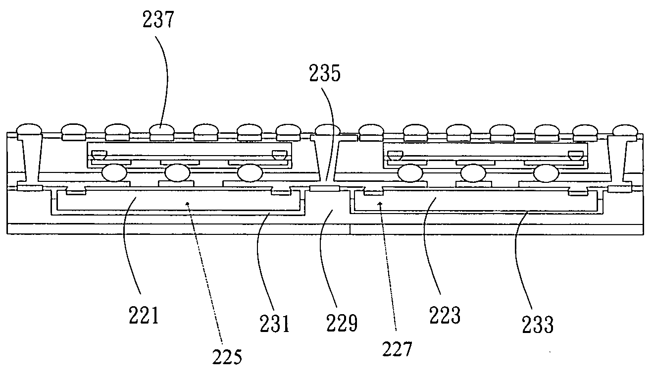
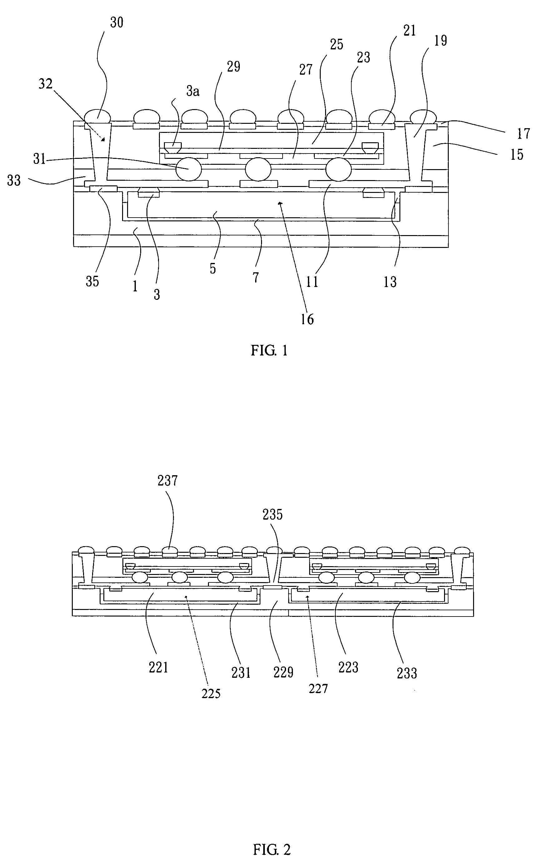
[0024]The present invention discloses a structure of Fan-out WLP having a substrate with at least a predetermined cavity and metal pads formed therein. FIG. 1 illustrates a cross-sectional view of panel scale package (PSP) for system in package (SIP) in accordance with one embodiment of the present invention. As shown in the FIG. 1, the structure of SIP includes a substrate 1 having a die receiving cavity 9 formed therein to receive at least the first die 5 with Al pads 3 (metal b...


PUM


Abstract

The present invention provides a structure of multi-chips package and Method of the same comprising a substrate with a pre-formed die receiving cavity formed within an upper surface of the substrate. A die is disposed within the die receiving cavity by adhesion and an elastic dielectric layer filled into a gap between the die and the substrate to absorb thermal mechanical stress; therefore the thickness of the package is reduced and the CTE mismatch of the structure is reduced. The present invention also provides a structure for SIP with higher reliability and lower manufacturing cost. the process is simpler and it is easy to form the multi-chips package than the traditional one. Therefore, the present invention discloses a fan-out WLP with reduced thickness and good CTE matching performance.

Description

FIELD OF THE INVENTION[0001]The present invention relates to a structure for system in Package (SIP), and more particularly to a panel scale package (PSP) with SIP.DESCRIPTION OF THE PRIOR ART[0002]In the field of semiconductor devices, the device density is increased but the device dimension is reduced. the traditional package technique, for example lead frame package, flex package, rigid package technique, can't meet the demand of producing smaller chip with high density elements on the chip; therefore, new packaging or interconnecting techniques for such high density devices become demanding.[0003]For the reasons mentioned above, the trend of package technique development is toward ball grid array (BGA), flip chip (FC-BGA), chip scale package (CSP), Wafer level package (WLP); wherein, WLP technique is an advanced packaging technology, by which the dice are packaged and tested on the wafer before performing singulating. Furthermore, WLP is such an advanced technique so that the pr...

Claims


Application Information

Patent Timeline
Patent Type & Authority Applications(United States)
IPC IPC(8): H01L23/48H01L21/00
CPCH01L23/13H01L24/19H01L25/0657H01L25/50H01L2225/06513H01L2225/06524H01L2225/06527H01L2225/06541H01L2924/09701H01L2224/12105H01L2224/16145H01L2224/24227H01L2224/32225H01L2224/73267H01L2224/92244H01L2924/15153H01L2924/10253H01L25/0652H01L2924/00H01L2224/05001H01L2224/05026H01L2224/05124H01L2224/05147H01L2224/05155H01L2224/05166H01L2224/05548H01L2224/05644H01L2224/05666H01L2924/351H01L2924/00014H01L2924/01029H01L2924/01079H01L2924/01055H01L23/12
Inventor YANG, WEN-KUNHSU, HSIEN-WENWU, YA-TZUHUANG, CHING-SHUN
Owner ADVANCED CHIP ENG TECH
Why Eureka
Try Eureka