Electrostatic discharge protection element having an improved area efficiency

a protection element and electrostatic discharge technology, applied in the field of electrostatic discharge protection elements, can solve the problems of gate oxide film, low electrostatic discharge protection performance, and limit the use of the diode independently, and achieve the effect of improving area efficiency

Inactive Publication Date: 2008-08-21
SK HYNIX INC
View PDF8 Cites 12 Cited by
  • Summary
  • Abstract
  • Description
  • Claims
  • Application Information

AI Technical Summary

Benefits of technology

[0010]Therefore, the present invention provides an electrostatic discharge protection element that im

Problems solved by technology

However, there is a limitation in using the diode independently since a reverse turn-on voltage is high and electrostatic discharge protection performance is low in a reverse direction condition.
The SCR discharges a high amount of current per unit area, though it has a problem where a gate oxide film of the semiconductor internal element can be damaged before the electrostatic discharge protection element operates when the electrostati

Method used


Image

  • Electrostatic discharge protection element having an improved area efficiency
  • Electrostatic discharge protection element having an improved area efficiency
  • Electrostatic discharge protection element having an improved area efficiency

Examples


Embodiment Construction

[0026]Hereinafter, embodiments of the present invention will be described in detail with reference to the accompanying drawings.

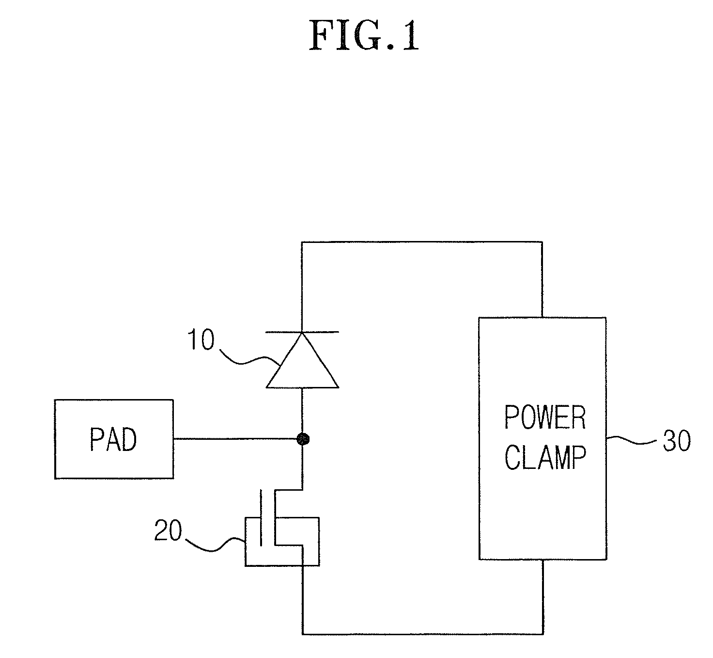
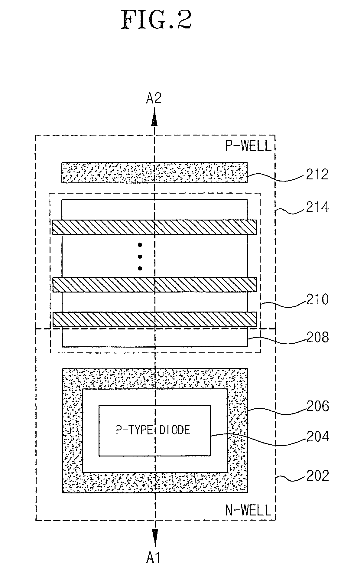
[0027]The present invention is related to an electrostatic discharge protection element that reduces a distance between a diode and a power clamp and improves area efficiency by embedding the power clamp within the diode and the GGNMOS transistor. An embodiment of the present invention will be described referring to FIG. 2.

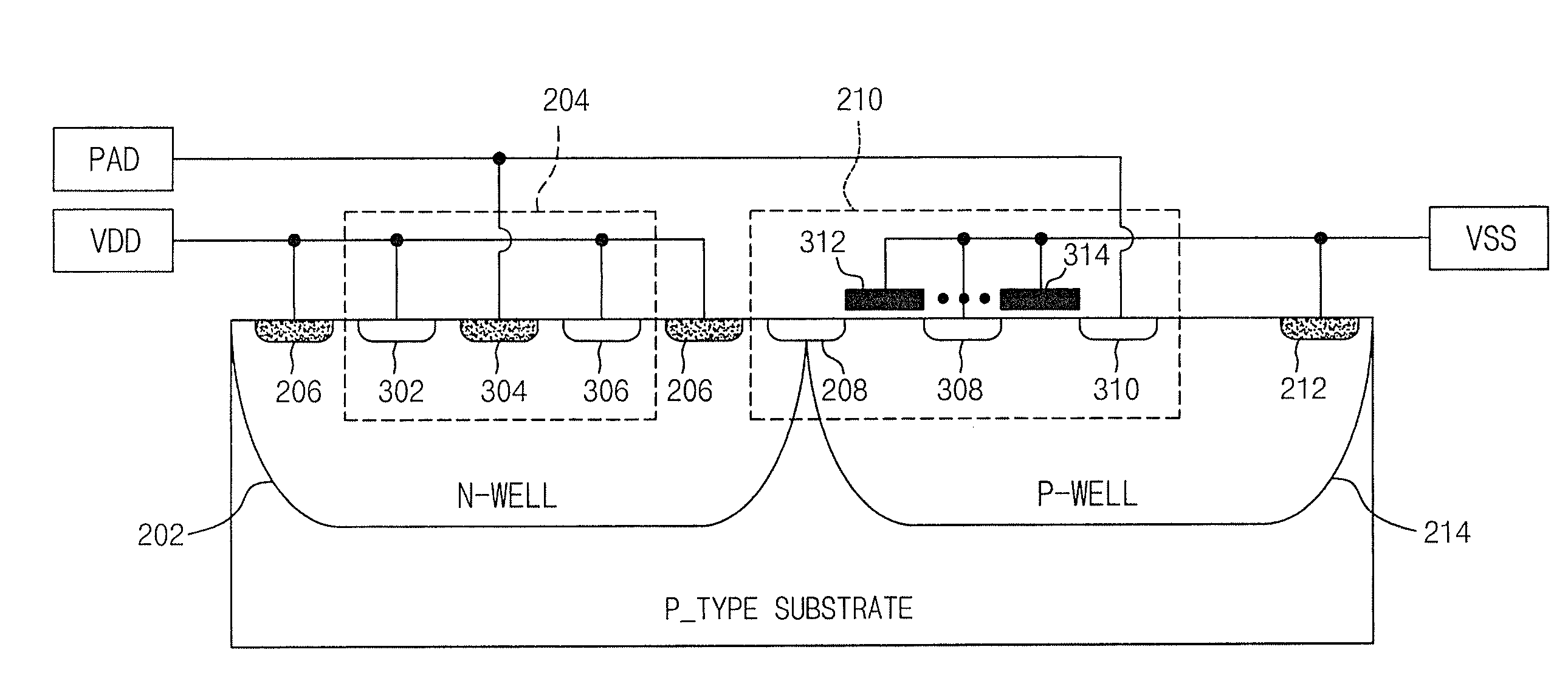
[0028]Referring to FIG. 2, the electrostatic discharge protection element according to an embodiment of the present invention includes a P-type diode 204 formed within an N-well region 202 and a GGNMOS transistor 210 formed across the N-well region 202 and a P-well region 214.

[0029]A P-type impurity region 206 is formed within the N-well region 202 by a prescribed distance surrounding the P-type diode 204 to serve as an anode of a low voltage silicon-controlled rectifier (LVTSCR). Additionally, a P-type guard ring 212 is formed within the...


PUM


Abstract

An electrostatic discharge protection element is disclosed for protecting an internal circuit from electrostatic current. The electrostatic discharge protection element forms an embedded LVTSCR by adding a prescribed impurity region within an N-well region having a P-type diode formed therein. A P-well region having a GGNMOS transistor is also formed in the electrostatic discharge protection element. The embedded LVTSCR improves area efficiency, reduces a resistance, and lowers an operational voltage by reducing the distance between the P-type diode and the LVTSCR to allow high-speed operatation.

Description

CROSS-REFERENCE TO RELATED APPLICATIONS[0001]The present application claims priority to Korean patent application number 10-2007-0016256 filed on Feb. 15, 2007, which is incorporated herein by reference in its entirety.BACKGROUND OF THE INVENTION[0002]The present invention relates generally to a semiconductor memory device, and more particularly to an electrostatic discharge protection element that protects an internal circuit from an electrostatic current.[0003]Generally, a semiconductor memory device has an electrostatic discharge protection element provided between an input / output pad and the internal circuit. The electrostatic discharge protection element serves to prevent damage to the internal circuit resulting from electrostatic current flowing in from a charged body or machine to the inside of the semiconductor memory device, or the electrostatic current flowing out through the machine after being charged within the semiconductor memory device.[0004]The electrostatic dischar...

Claims


Application Information

Patent Timeline
IPC IPC(8): H02H9/00H01L27/06
CPCH01L27/0262H01L23/60H01L27/04
Inventor LIM, DONG JU
Owner SK HYNIX INC
Why Eureka
Try Eureka