Embedded architecture with serial interface for testing flash memories

Inactive Publication Date: 2008-08-21
ATMEL CORP
View PDF70 Cites 10 Cited by
  • Summary
  • Abstract
  • Description
  • Claims
  • Application Information

AI Technical Summary

Benefits of technology

[0012]The present invention aims at reducing the testing time of flash memories by combining a serial interface to increase the number of dice tested in parallel, without over increasing the total number of wires on the probe card (which will be refe

Problems solved by technology

As technology features scale down and flash memory densities grow larger, the total number of interactions increase between the external tester and the flash memory during the array sc

Method used


Image

  • Embedded architecture with serial interface for testing flash memories
  • Embedded architecture with serial interface for testing flash memories
  • Embedded architecture with serial interface for testing flash memories

Examples


Embodiment Construction

[0020]Persons of ordinary skill in the art will realize that the following description of the present invention is illustrative only and not in any way limiting. Other embodiments of the invention will readily suggest themselves to such skilled persons.

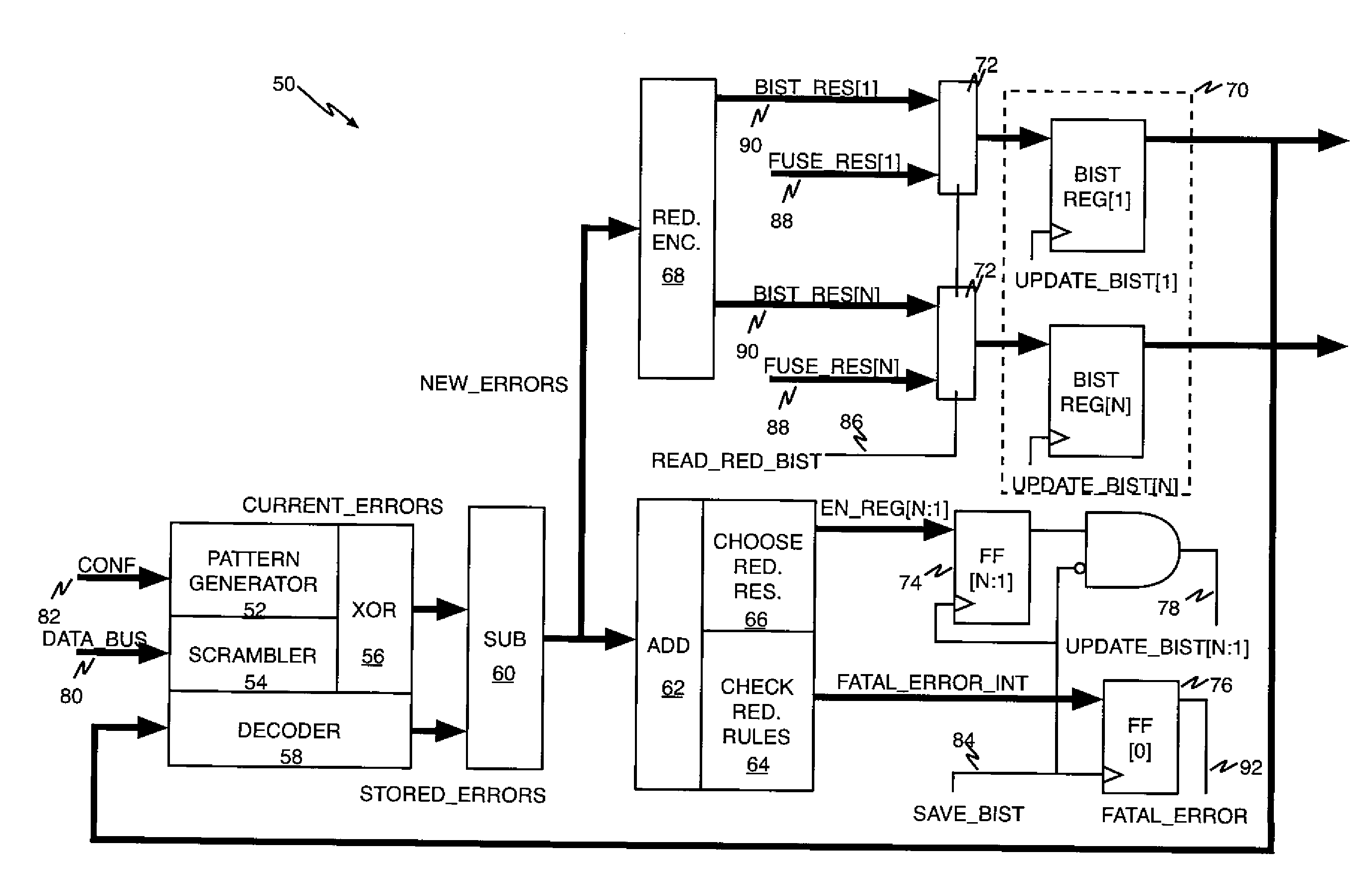
[0021]The architecture of the present invention can be extended to chips with N redundancy resources made of K bits, where N is the number of redundancy resources available on the device and K is the number of bits needed to completely describe a single resource.

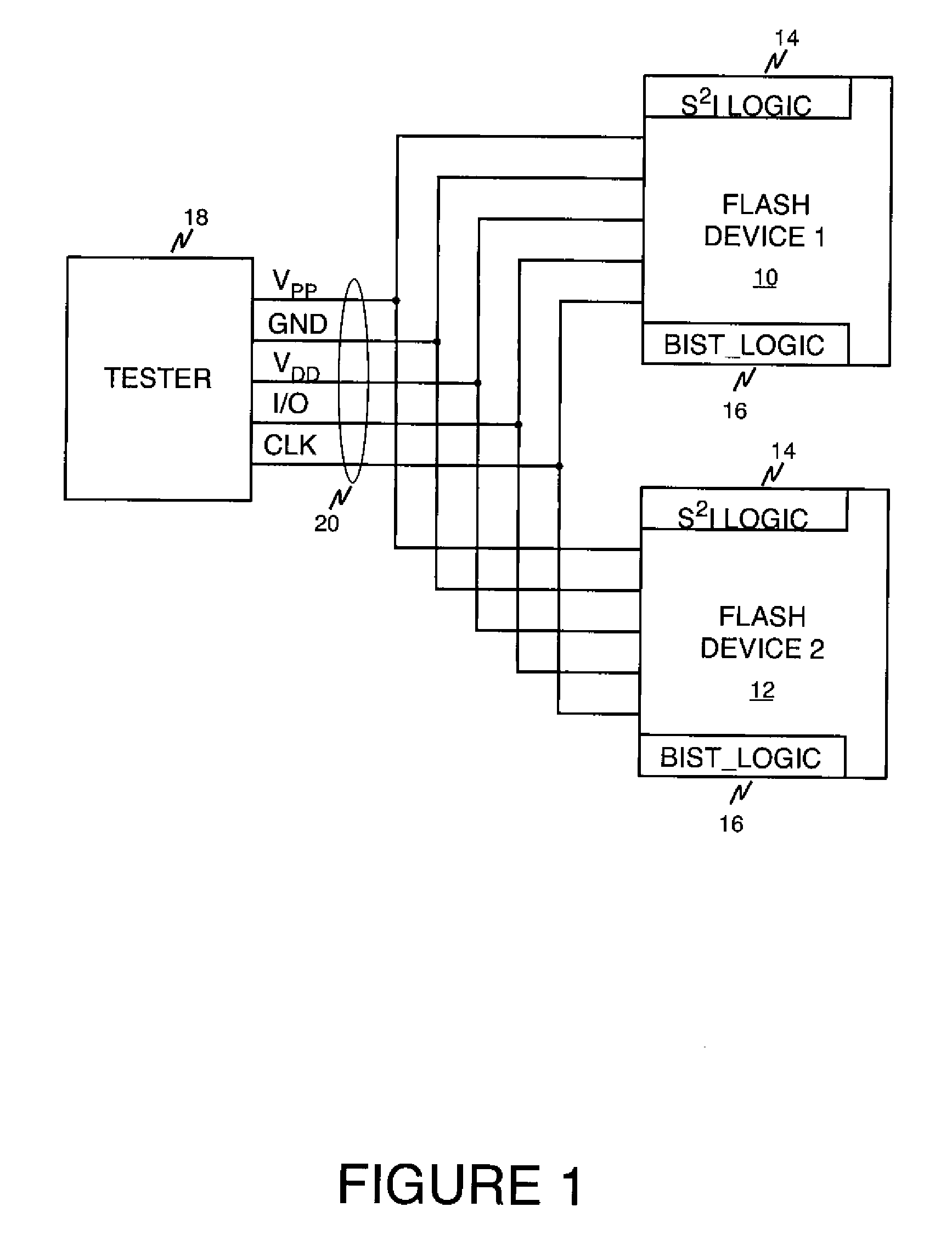
[0022]Referring now to FIG. 1, a block diagram shows two flash memory devices 10 and 12 configured according to the principles of the present invention and including a S2I_logic block 14 and a BIST logic block 16. Flash memory devices 10 and 12 are coupled to a tester 18 via a 5-wire bus 20. The 5-wire bus 20 includes VPP, a potential that may be used to program the flash memory devices 10 and 12, VDD to supply the standard power for the flash memory devices 10 and 12, GND, to...


PUM


Abstract

A flash memory device includes a flash memory array, a set of non-volatile redundancy registers, a serial interface, and testing logic coupled to the serial interface, the testing logic configured to accept a set of serial commands from an external tester; erase the array; program the array with a test pattern; read the array and compare the results with expected results to identify errors; determine whether the errors can be repaired by substituting a redundant row or column of the array, and if so, generate redundancy information; and program the redundancy information into the non-volatile redundancy registers.

Description

BACKGROUND OF THE INVENTION[0001]1. Field of the Invention[0002]The present invention pertains to testing circuitry for flash memories, and to improvements in the time needed to screen flash memory arrays. More particularly, the present invention pertains to flash memory integrated circuits with on-board testing circuitry.[0003]2. The Prior Art[0004]It is well known that screening a flash array accounts for the majority of the time spent during flash memory testing. Flash array screening usually consists of a sequence of erasing the array, programming the array with a pattern, and reading and verifying the pattern written into the array. If the programmed pattern can be verified, then the array is assumed to be defect free, otherwise, if errors occur, some defects have been detected. Repeating the sequence with different patterns allows for the highlighting of different types of faults.[0005]Thus, a key point in testing the array is determining whether or not the defects can be repa...

Claims


Application Information

Patent Timeline
IPC IPC(8): G11C7/00
CPCG11C16/04G11C29/1201G11C29/16G11C2029/3602G11C29/4401G11C29/789G11C29/32
Inventor REGGIORI, RICCARDO RIVATASSAN CASER, FABIOMARSELLA, MIRELLAMARZIANI, MONICA
Owner ATMEL CORP
Why Eureka
Try Eureka