Semiconductor device including conductive lines with fine line width and method of fabricating the same

a technology of conductive lines and semiconductor devices, which is applied in the direction of semiconductor devices, semiconductor/solid-state device details, electrical apparatus, etc., can solve the problems of increasing the difficulty of disposing interconnection increasing the difficulty of disposing bit lines and word lines required for operating cell transistors, and the size of cell transistors being continually reduced

Active Publication Date: 2008-08-28
SAMSUNG ELECTRONICS CO LTD
View PDF3 Cites 10 Cited by
  • Summary
  • Abstract
  • Description
  • Claims
  • Application Information

AI Technical Summary

Benefits of technology

[0009]One aspect of the present disclosure includes a semiconductor device. The device comprises a semiconductor substrate including a first core region and a second core region between which a cell array region is interposed, a first conductive line and a second conductive line extending to the first core region across the cell array region, and a third conductive line and a fourth conductive line extending to the second core region across the cell array region, wherein a line width of the first through fourth conductive lines is smaller than a resolution limit in a lithography process.

Problems solved by technology

However, with a reduction in size of the cell transistor, it is increasingly difficult to dispose interconnection lines required for operating the cell transistor.
That is, it is increasingly difficult to dispose bit lines and word lines required for operating a cell transistor as the size of the cell transistor is being continually reduced.
However, Aratani suffers from a number of limitations.
For example, because the word lines extend only in one direction from the memory cell array region, when the word lines have a line width smaller than the resolution limit in a lithography process, it may be difficult to secure a region for the contact region of the word lines.

Method used


Image

  • Semiconductor device including conductive lines with fine line width and method of fabricating the same
  • Semiconductor device including conductive lines with fine line width and method of fabricating the same
  • Semiconductor device including conductive lines with fine line width and method of fabricating the same

Examples


first embodiment

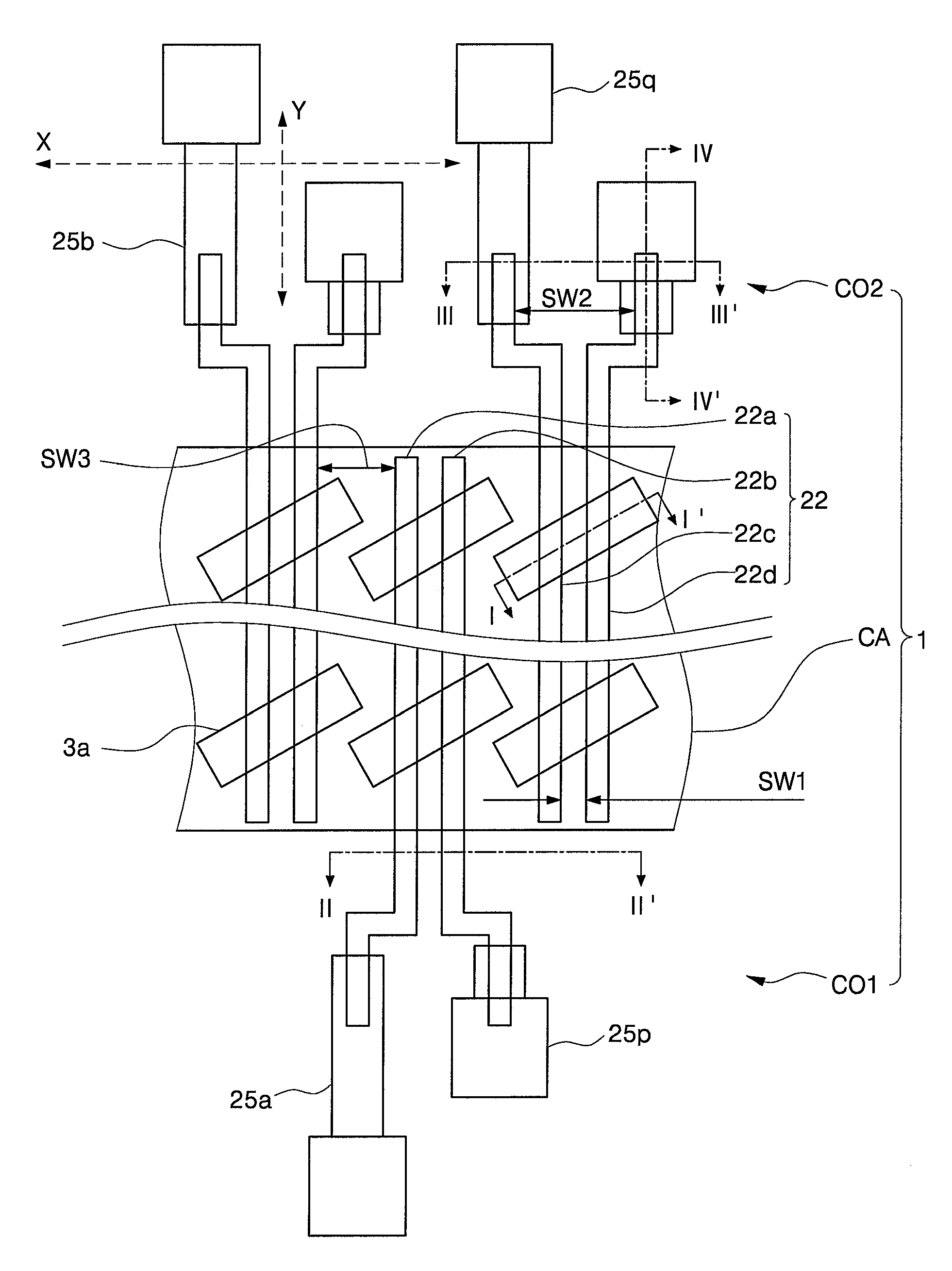
[0045]As described above, the conductive lines 122 according to the above-described exemplary embodiment extend in the first and second core regions CO1 and CO2 by different lengths from the conductive lines 22 according to the present invention. Also, the contact pads 125p and 125q of this embodiment may be on substantially the same level as the contact pads 25p and 25q of the previously embodiment in the first and second core regions CO1 and CO2.

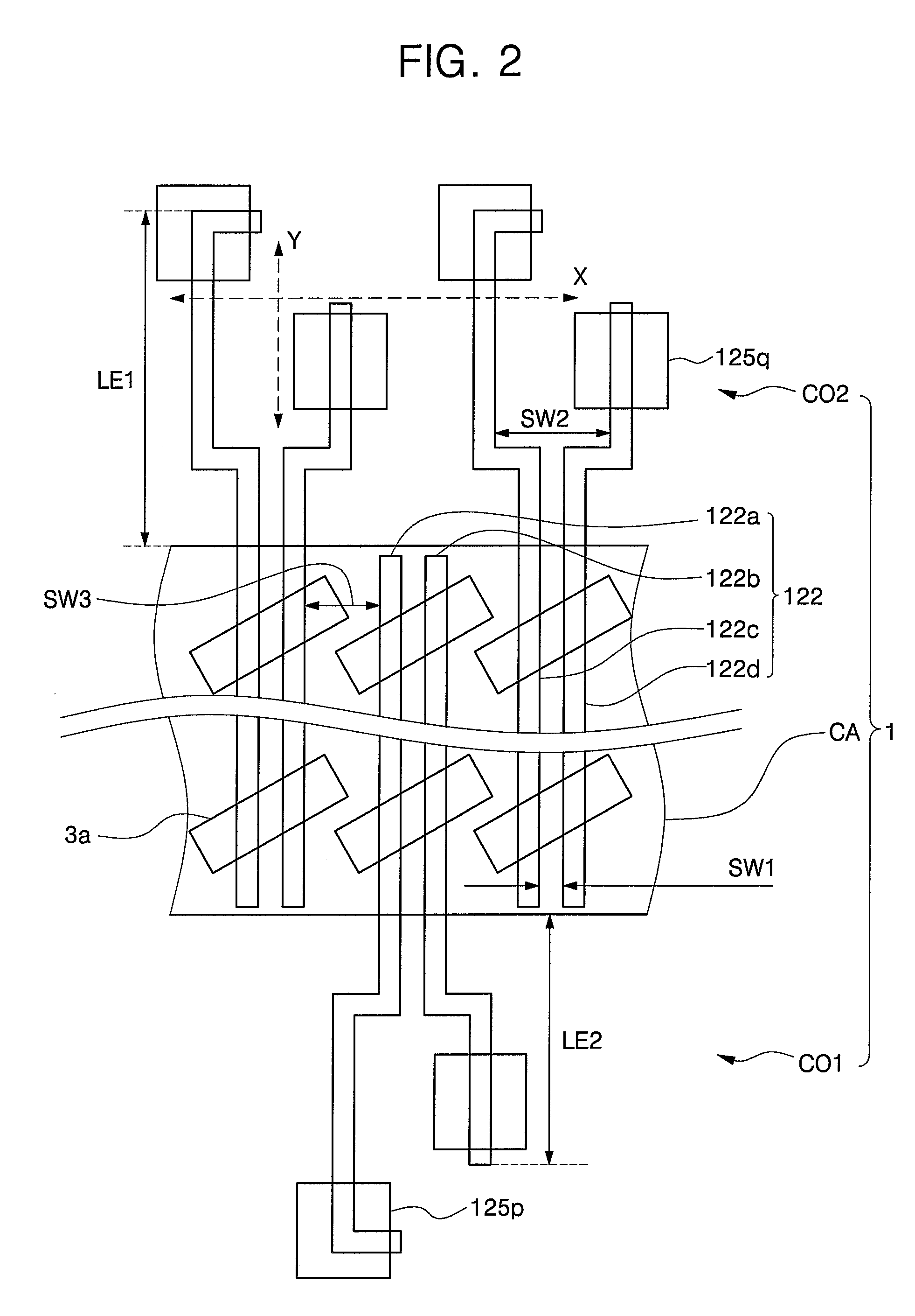
[0046]FIG. 3 represents an alternative structure and method for disposing conductive lines across an active cell region. Specifically, in FIG. 3, each of the conductive lines 222 has a greater line width in the first core region CO1 or the second core region CO2 than in the cell array region CA.

[0047]Still referring to FIG. 3, the conductive lines 222 may include first, second, third, and fourth conductive lines 222a, 222b, 222c, and 222d that are arranged in sequence. In the cell array region CA, the conductive lines 222 may have a first ...

third embodiment

[0049]First and second contact pads 225p and 225q may be electrically connected to end portions of the conductive lines 222 that have the second line width LW2. Furthermore, similar to a previously disclosed exemplary embodiment, the first and second contact pads 225p and 225q may be on substantially the same level. Therefore, connection portions 225a may be provided between the contact pads 225p and the end portions of the conductive lines 222 like a previously disclosed embodiment. As described above, the conductive lines 222 of the third embodiment have a different line width from the conductive lines 22 in a previously disclosed embodiment in the first and second core regions CO1 and CO2. As a result, in the present embodiment, an electrical characteristic between the conductive lines 222 and the contact pads 225p can be improved.

[0050]In yet another exemplary embodiment, the conductive lines 222 described above are disposed in a manner such that the connection portions 225a are...


PUM


Abstract

A semiconductor device comprises a semiconductor substrate including a first core region and a second core region between which a cell array region is interposed, a first conductive line and a second conductive line extending to the first core region across the cell array region, and a third conductive line and a fourth conductive line extending to the second core region across the cell array region, wherein a line width of the first through fourth conductive lines is smaller than a resolution limit in a lithography process.

Description

[0001]A claim of priority is made to Korean Patent Application No. 10-2006-0097266, filed on Oct. 2, 2006, the contents of which are hereby incorporated herein by reference in their entirety.BACKGROUND OF THE INVENTION[0002]1. Field of the Invention[0003]The present disclosure relates to a semiconductor device and a method of fabricating the same and, more particularly, to a semiconductor device including conductive lines with a fine line width and a method of fabricating the same.[0004]2. Description of Related Art[0005]In recent years, as the demand for smaller sized electronic appliances increases, an increasing number of methods for increasing the integration density of semiconductor devices are being developed. These methods include not only techniques for reducing the size of components of the semiconductor devices, but also techniques for efficiently disposing components of the semiconductor devices on surfaces such as, for example, a semiconductor substrate. For example, a s...

Claims


Application Information

Patent Timeline
Patent Type & Authority Applications(United States)
IPC IPC(8): H01L23/522H01L21/768
CPCH01L21/743H01L27/10897H01L27/10882H01L27/105H10B12/48H10B12/50H10B99/00
Inventor SEO, HYEOUNG-WONROH, BYUNG-HYUGKIM, SEONG-GOOJEON, SANG-MIN
Owner SAMSUNG ELECTRONICS CO LTD
Why Eureka
Try Eureka