Programmable Logic Device

a logic device and programmable logic technology, applied in the field of programmable logic devices, can solve the problems of difficult performance estimation of logic circuits, difficult to predict interconnection delay, time-consuming work, etc., and achieve the effect of increasing the number of levels of lut cascade, and increasing the degree of freedom for design

Inactive Publication Date: 2008-08-28
KITAKYUSHU FOUND FOR THE ADVANCEMENT OF IND
View PDF2 Cites 10 Cited by
  • Summary
  • Abstract
  • Description
  • Claims
  • Application Information

AI Technical Summary

Benefits of technology

[0027]The logic function in the memory for logic and the information for connection in the memory for interconnections are updated so that the LUT cascade realizes the objective function. In this case, we can change the number of rail outputs (that is, the number of lines that connect two adjacent memories for logic), and the number of external input lines that are connected to the memory for logic. In this way, we can compose the LUT cascade that realizes objective logic function. That is, we can adjust the number of rails and the number of external input variables that are connected to the memory for logic in the succeeding stage. In this way, with a single PLD, we can realize wide range of logic functions. As a result, we can reduce the number of input lines of the memory for logic. And, we can reduce the size of the circuit.
[0074]In many of practical LUT cascades, to at least one input line of the memory for logic, the output of the memory for logic in the preceding stage is connected. Thus, we can implement a general-purpose PLD, where in the memory for logic other than the first stage, at least one of the outputs of the memory for logic in the preceding stage is directly connected to the input of the memory for logic of the succeeding stage without passing through the interconnection circuit. With this design, the number of input lines of the interconnection circuit can be reduced. Moreover, we can reduce the size of the circuit further, because we can reduce the interconnection circuit and the number of wiring in the memory for interconnections.

Problems solved by technology

Therefore, the physical design to reduce interconnection delay is necessary, and such work is a time-consuming work.
Moreover, since the delay depends on interconnections between CLBs, the interconnections delay is hard to predict without finishing the layout.
Therefore, the performance estimation of the logic circuits is difficult during logic design.
Moreover, since pass transistors are used for the interconnections, the delay of the interconnection part is fairly large.
Thus, the chip area of FPGA tends to be large.
Therefore, the operation speed of an LUT cascade can be slower than an optimally designed FPGA.
But, this is not so convenient.
Therefore, such strategy will increase unused memory.
And, the compact implementation will be difficult, and the power consumption increase, too.

Method used


Image

  • Programmable Logic Device
  • Programmable Logic Device
  • Programmable Logic Device

Examples


embodiment 1

II. Embodiment 1

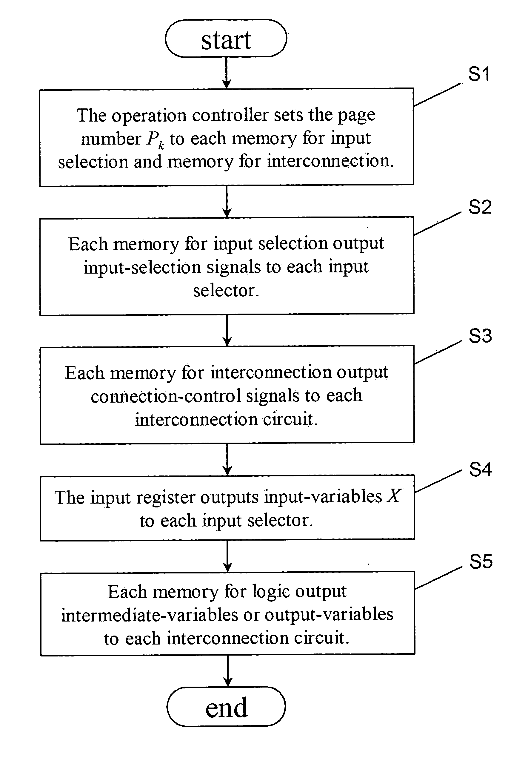
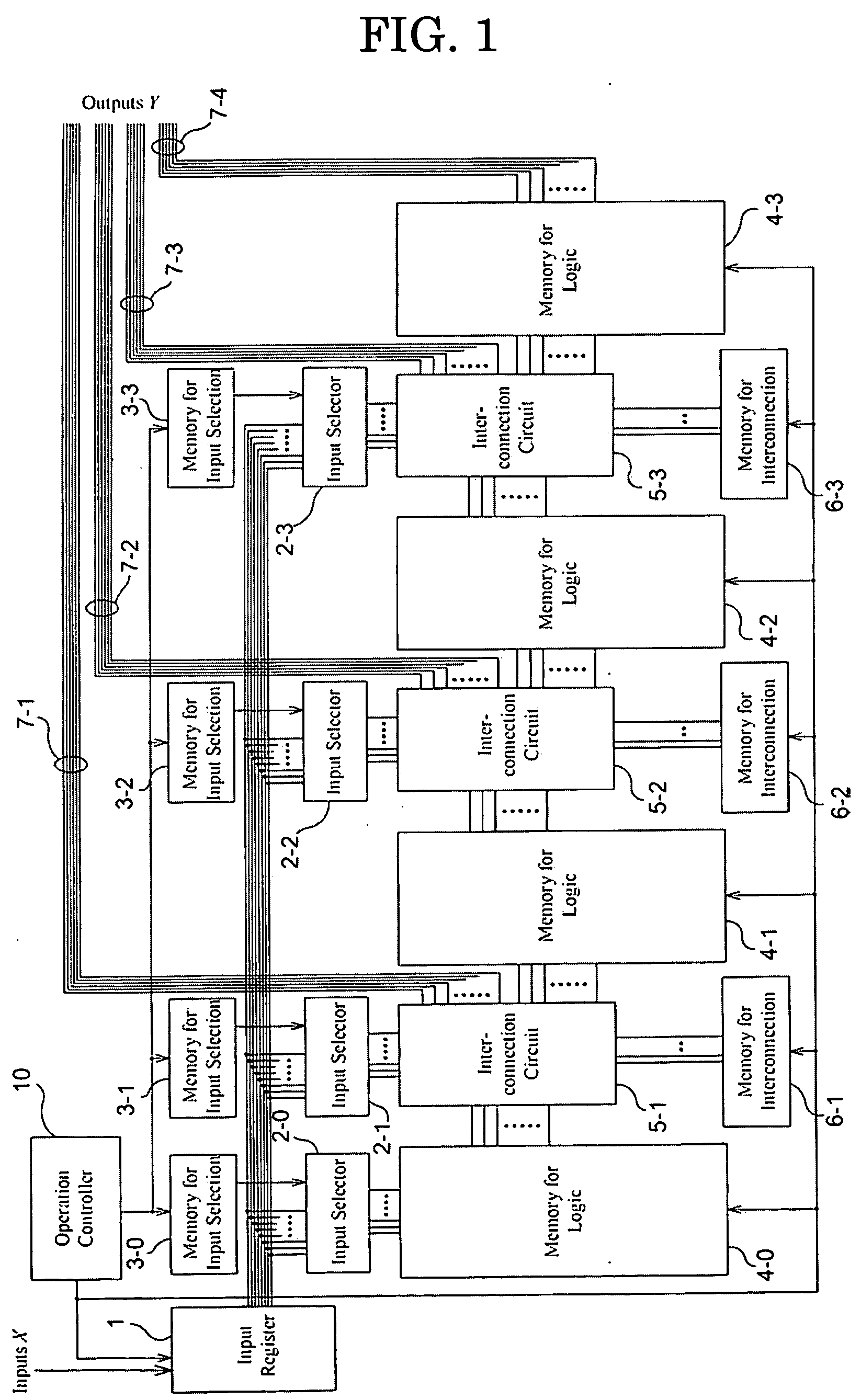
[0144]The simplified block diagram of the PLD in accordance with EMBODIMENT 1 of the present invention is illustrated in FIG. 1.

[0145]The PLD for EMBODIMENT 1 of the present invention consist of an input variable register (1); input selectors (2-0)-(2-3); memories for input selection (3-0)-(3-3); memories for logic (4-0)-(4-3); interconnection circuits (5-1)-(5-3); memories for interconnections (6-1)-(6-3); and an operation control part (10).

[0146]The input variable register (1) stores the inputs X=(x1, . . . , xn): where X has n variables, and is used for the operation of objective logic function ƒ(X), where n is a natural number. Input variables X are sent through the external input lines to the input variable register (1). Memories for logic (4-0)-(4-3) store the truth tables of decomposition functions {ƒi; iε{0, 1, 2, 3}}: where they are obtained by decomposing the objective logic function ƒ, and are stored as LUTs. In this embodiment, the number of stages of the...

example 1

(End of Example 1)

III. Embodiment 2

[0215]The simplified block diagram of the PLD in accordance with EMBODIMENT 2 of the present invention is illustrated in FIG. 17.

[0216]The feature of this EMBODIMENT is as follows: a part of the output lines of the input selectors (2-1)-(2-3) are directly connected to the inputs of memories for logic (4-1)-(4-3) without using the interconnection circuits (5-1)-(5-3). In many practical logic functions, at least one external input variable is connected to an input of the memories for logic (4-1)-(4-3). That is, at least one output line of the input selectors (2-1)-(2-3) is often connected to the input of the memories for logic (4-1)-(4-3). Therefore, in a PLD used in practice, if a part of the output lines of input selectors (2-1)-(2-3) is connected directly to the input of memories for logic (4-1)-(4-3) without using the interconnection circuits (5-1)-(5-3), then we can decrease the number of the input lines of the interconnection circuits (5-1)-(5-...

embodiment 3

IV. Embodiment 3

[0217]The simplified block diagram of the PLD in accordance with EMBODIMENT 3 of the present invention is illustrated in FIG. 18.

[0218]The first feature of this EMBODIMENT is that the PLD has; the input selectors (30-1)-(30-3) that select the input variables, and send them directly into the memories for logic (4-1)-(4-3) without using the interconnection circuits (5-1)-(5-3) and the memories for input selection (31-1)-(31-3) that stores the information for the connection of the input selectors (30-1)-(30-3); in addition to the input selectors (2-1)-(2-3) that select the input variables and send them to the interconnection circuits (5-1)-(5-3). Moreover, the second feature of this EMBODIMENT is that in this PLD, a part of the intermediate variables is directly connected from the output of the memory for logic (4-(i−1)) (iε{1, 2, 3}) in the preceding stage, to the memory for logic (4-i) of succeeding stage, without using the interconnection circuits (5-1)-(5-3).

[0219]B...


PUM


Abstract

The invention relates to a connector (10) for connecting welding torch where the connector comprises a connector body (12) made of electrically insulating material, a cylindrical current transferring body (30) fitted on the cylindrical front part (13) of the connector body (12), made of electrically conductive material, where the current transferring body (30) has a threaded surface (32) and a side contact surface (35) besides the threaded surface (32) on its side surface, a threaded bore (37) on the side contact surface (35) for fixing current cable with screwed joint and a frontal contact surface (33), further an attachment bracket (60), made of electrically insulating plastic, the attachment bracket (60) has a sleeve part (62), which encircles space apart the threaded surface (32) and the sleeve part (62) has a flange (64) protruding from its front part for fixing, the flange (64) is provided with one or more holes (65) in it. The connector body (12) has a rear limiting surface (18) out of which a stem (75) projects, the stem (75) has a bore hole (77) in its centre line into which a liner (54) for wire guide is fixed, which liner leads in a nest (21) for fitting wire guide conduit end formed on the front surface (15) of the connector body (12), the current transferring body (30) has a pot-shape, having a bottom (39) in which there are openings (41, 42, 43) opening onto the nests (21, 23) formed on the front surface (15), further there is a positioning hole (27) in the side of the connector body (12) in the extension of the threaded bore (37) and the attachment bracket (60) has a conically narrowed part (68) projecting rearwards from the sleeve part (62), and on the inner surface near the end of the narrowed part (68) there is at least one screw thread (72) which The invention relates to a connector (10) for connecting welding torch where the connector comprises a connector body (12) made of electrically insulating material, a cylindrical current transferring body (30) fitted on the cylindrical front part (13) of the connector body (12), made of electrically conductive material, where the current transferring body (30) has a threaded surface (32) and a side contact surface (35) besides the threaded surface (32) on its side surface, a threaded bore (37) on the side contact surface (35) for fixing current cable with screwed joint and a frontal contact surface (33), further an attachment bracket (60), made of electrically insulating plastic, the attachment bracket (60) has a sleeve part (62), which encircled space apart the threaded surface (32) and the sleeve part (62) has a flange (64) protruding from its front part for fixing,—the flange (64) is provided with one or more holes (65) in it. The connector body (12) has a rear limiting surface (18) out of which a stem (75) projects, the stem (75) has a bore hole (77) in its centre line into which a liner (54) for wire guide is fixed, which liner leads in a nest (21) for fitting wire guide conduit end formed on the front surface (15) of the connector body (12), the current transferring body (30) has a pot-shape, having a bottom (39) in which there are openings (41, 42, 43) opening onto the nests (21, 23) formed on the front surface (15), fu

Description

TECHNICAL FIELD[0001]This invention is related to the programmable logic device (PLD). More particularly, this invention is related to the architecture, operation and design of PLD that utilizes lookup table cascade (LUT cascade), where each LUT corresponds to the decomposed function of the objective logic function.BACKGROUND ART[0002]Field programmable gate arrays (FPGAs) are widely used in the design of the logic circuits, recently (reference 1). An FPGA is a PLD that can change interconnections among logic cells (Configurable Logic Block: CLB) arranged in a two-dimensional matrix by rewriting the memory. FPGAs work as hardware, and are different from microprocessors (MPUs) that operate software programs. Thus, a feature of FPGAs is their fast manipulation of logic functions.[0003]On the other hand, in FPGAs, we can change physical interconnections between CLBs by programming. Therefore, the physical design to reduce interconnection delay is necessary, and such work is a time-cons...

Claims


Application Information

Patent Timeline
Patent Type & Authority Applications(United States)
IPC IPC(8): G06F7/38G06F7/00H03K19/177
CPCH03K19/17728H03K19/17784H03K19/1776H03K19/17736G05B19/00G06F7/00
Inventor SASAO, TSUTOMUIGUCHI, YUKIHIRO
Owner KITAKYUSHU FOUND FOR THE ADVANCEMENT OF IND
Why Eureka
Try Eureka